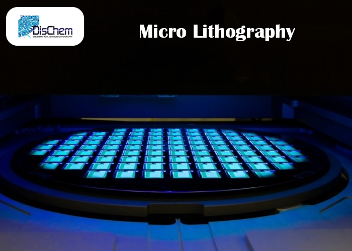
Why E-Beam Lithography Systems Matter in AI Chip Manufacturing?
Jun 12, 2026
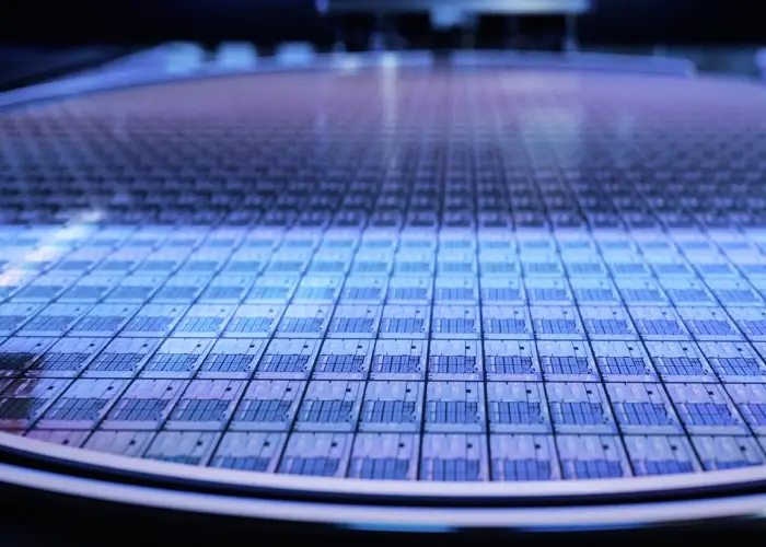
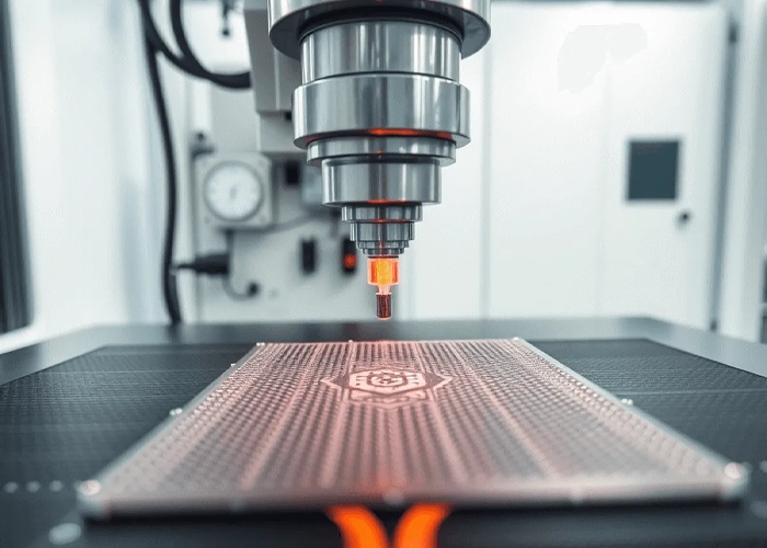
An e beam lithography system is a very important tool for making artificial intelligence (AI) chips. It works like a super-fine pen. It uses a tight beam of electrons to draw tiny lines and patterns directly onto a coated surface. AI chips need billions of tiny switches packed close together to work. This system helps […]
Hydrogen Silsesquioxane, commonly known as HSQ negative resist, is a special glass-like liquid used in technology to create tiny patterns on computer chips. It is the top choice for high-resolution electron beam lithography because it lets engineers draw lines thousands of times thinner than a human hair. When hit by an electron beam, this liquid […]
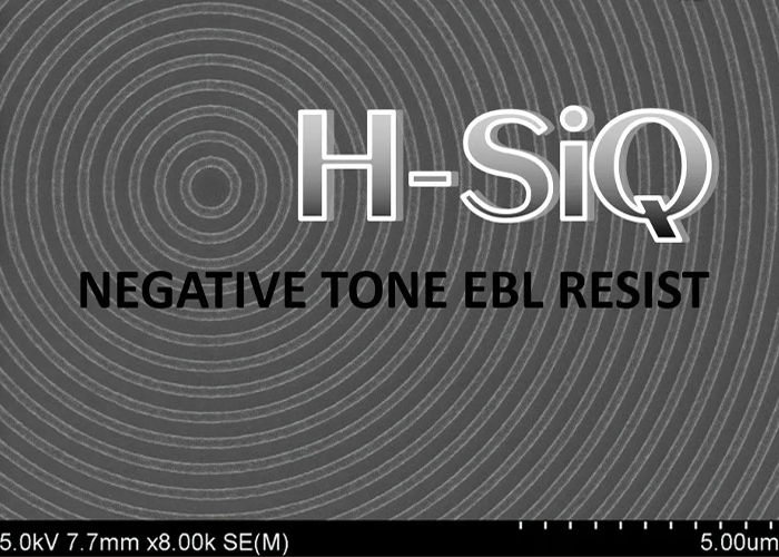
Hydrogen Silsesquioxane (HSQ) electron-beam resist is a high-quality glass-like coating used in microchip making to create tiny patterns smaller than 10 nanometers. It is a silicon-based material that starts as a liquid. When a beam of electrons hits the surface, it triggers a chemical change that turns the material into a hard, solid layer similar […]
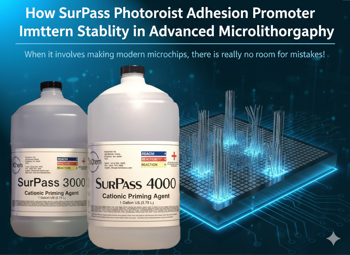
When it involves making modern microchips, there is really no room for mistakes! As we try to make features smaller and smaller, keeping everything stable on the wafer is a huge deal for engineering teams. Making sure the photoresist actually stays stuck to the surface isn’t just a nice extra. It is a total requirement […]
Electron beam charge dissipation is the process of neutralizing or removing built up static electricity from a surface during the making of tiny electronic parts. By providing a path for electricity to flow, this method stops negative particles from gathering and pushing the electron beam off course. Using a reliable electron beam charge dissipation strategy […]
Making high-tech electronics takes a lot of care and steady hands at every turn. In the world of advanced manufacturing, small details lead to huge results. DisChem Inc. has the smart chemical tools that is SurPass microlithography adhesion, which makes this kind of accuracy a total breeze! One of the biggest secrets to success is […]
Electron beam lithography plays a vital role in advanced manufacturing environments where ultra-high resolution and precise pattern control are required. It is widely used for applications such as mask writing, nanofabrication, photonics, and exploratory research in next-generation devices. The e-beam lithography system enables feature sizes that extend far beyond the limits of traditional optical lithography, […]
High-resolution electron beam lithography is a cornerstone of advanced manufacturing technologies, supporting applications that range from holograms and optical media to microlithography and next-generation nanofabrication. As feature sizes shrink and pattern complexity increases, controlling defects becomes increasingly challenging. One of the most common and disruptive sources of defects in these environments is surface charging. Effective […]

In advanced lithographic manufacturing, achieving flawless coatings is not just a goal; it is a necessity. Whether producing holograms, optical media, microlithography devices, or e-beam manufactured components, uniform coatings and strong adhesion directly influence product yield, operational efficiency, and overall cost. A small defect in the coating process can result in delamination, pattern distortion, or […]
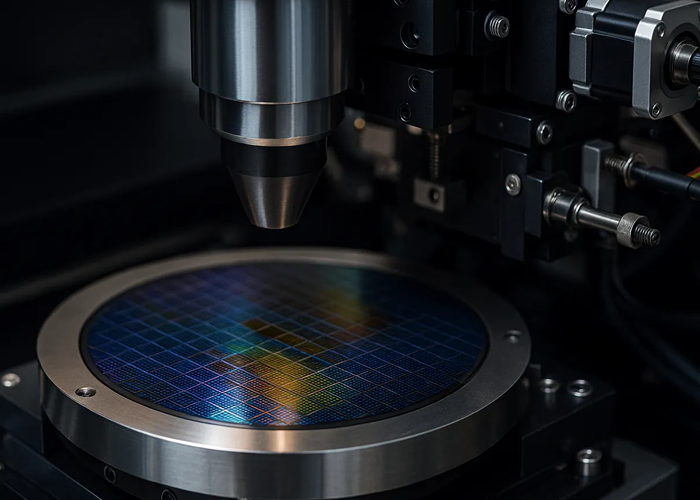
In a laboratory buzzing with the hum of electron-beam systems, engineers hover over microscopes, scrutinizing patterns invisible to the naked eye. Every line, every gap, every edge could make the difference between a device that performs flawlessly and one that fails at scale. This is the world of nanoscale fabrication, a world where precision is […]
In modern microfabrication, working at the nanometer scale means that even the smallest variation can define the success or failure of a device. Engineers in semiconductors, MEMS, and photonics operate in a domain where precision is paramount, and minor deviations can have cascading consequences. Substrate inconsistencies resist adhesion failures, and subtle differences in exposure conditions […]
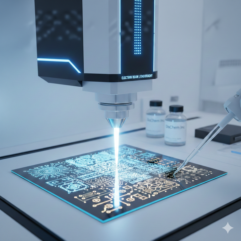
In the fast-evolving world of nanotechnology and microfabrication, electron beam lithography systems (e beam lithography system) are indispensable tools. These systems enable the creation of ultra-fine patterns essential for semiconductor devices, photonics, and advanced sensors. However, one critical challenge that often impacts the precision of these systems is surface charging during the lithography process. That’s […]
Quick Review Micro- and nanofabrication have changed faster in the last five years than in the previous twenty. We as manufacturers, researchers, and process engineers know that “close enough” is no longer good enough. Today’s production pipelines demand not just speed but atomic-level accuracy - all while keeping costs and waste under control. At DisChem Inc., we’ve […]
Quick Review Metal finishing is critical in nearly every modern manufacturing sector. We all want products that are durable, consistent, and reliable-for everything from electronics to aerospace components. Yet, achieving these goals is not always straightforward. Problems like uneven thickness, pinholes, and limited reproducibility can quickly derail quality or add cost. At DisChem Inc., we […]

Leaders in electronics, photonics, and advanced manufacturing are feeling the pressure to innovate faster and on a smaller scale. Devices are getting tinier, more complex, and demand for reliability has never been higher. Enter the e beam lithography system, a game-changing technology that puts precision and adaptability at the heart of your R&D and production. […]

Achieving true nanoscale precision remains one of the great challenges, and opportunities, facing manufacturers and R&D teams across electronics, photonics, and advanced materials. Electron beam nanolithography (EBN), also known as EBL, stands out for its ability to create astonishingly small features, unlocking new possibilities in quantum devices, medical tech, and semiconductor innovation. But for many, […]

Quick Review The market for advanced microfabrication is pushing its limits. Every R&D team and innovative manufacturer faces the challenge of creating complex, high-precision structures, sometimes with little room for prototyping. As the push for smaller, faster, and more functional devices continues, direct write electron beam lithography is under a fresh spotlight. Can it offer […]

Quick Review Manufacturers and R&D labs face high stakes with microfabrication. Yield, speed, and design flexibility impact everything from quantum chips to advanced photonics. As devices shrink and pattern fidelity tightens, does your patterning technology truly keep up? Here we review why an E beam lithography system is more than a niche tool, and why […]

Electron beam nanolithography is reshaping how industries approach nanoscale design. For businesses operating in high-stakes sectors like semiconductors, medical devices, and quantum computing, it’s no longer just about reducing feature sizes — it’s about improving repeatability, precision, and scalability. As capital-intensive sectors aim to optimize every dollar invested in R&D and production, the need for […]

Nickel electroforming is no longer a fringe option—it’s now a primary manufacturing method for sectors that rely on sub-micron precision and repeatability. From aerospace tooling to micro-electromechanical systems (MEMS), the ability to form complex geometries with exceptional structural integrity has made this process indispensable. For B2B decision-makers evaluating scalability, cost efficiency, and durability, nickel electroforming […]

This blog explores why hydrogen silsesquioxane EBL negative is rapidly becoming the resist of choice for business leaders and engineers seeking precision and reliability in nanofabrication. We’ll break down the science, the business case, and how DisChem Inc. supports your innovation journey. Why Does Nanofabrication Demand New Materials? Business leaders in microelectronics and nanotechnology face […]

Curious about how next-generation chips and quantum devices achieve their mind-boggling precision? This blog explores the E-beam lithography process, why it matters for business leaders, and how it’s powering innovation in nanotechnology. Why Should Business Leaders Care About E-Beam Lithography? Let’s get straight to the point: if you’re leading a company that relies on cutting-edge […]
Have you ever struggled with photoresist peeling, pattern distortion, or weak adhesion during the e-beam lithography process? One of the most critical but often overlooked aspects of successful lithography is negative photoresist adhesion. Poor adhesion can lead to pattern defects, reduced resolution, and processing failures, ultimately affecting the quality of nanoscale fabrication. What is a […]

How do semiconductor manufacturers and researchers achieve nanoscale precision when designing microchips, photonics, and MEMS devices? Traditional lithography methods often hit a resolution limit, but electron beam lithography (EBL) offers a way to push past these barriers. In this Blog, we will explore the electron beam lithography process, its advantages, applications, and key considerations for […]
This blog delves into the world of e-beam lithography, exploring its role in transforming nanofabrication. We’ll discuss how e-beam lithography systems offer unprecedented precision and flexibility, enabling the creation of complex nanostructures that are driving innovation in fields like quantum computing and nanophotonics. Introduction to E-Beam Lithography Imagine being able to draw intricate patterns on […]

This blog explores the transformative potential of the e-beam lithography process in nanofabrication. We’ll delve into its precision, flexibility, and real-world applications, highlighting why it’s a crucial technology for advancing fields like quantum computing and nanophotonics. Introduction to Nanofabrication What about creating devices so small that they’re measured in nanometers? Welcome to the world of […]

We at DisChem Inc. are thrilled to announce our participation in the upcoming Electron, Ion, and Photon Beam Technology and Nanofabrication (EIPBN) conference in Savannah, Georgia, from May 27-30, 2025. As a proud sponsor of this cutting-edge event, we’re gearing up to showcase our latest innovations in chemical solutions for advanced lithography. Our team is […]

This blog will discuss in detail about the importance of electron beam nanolithography, its current challenges, and how innovative solutions such as DisCharge, an anti-charging agent, are shaping the future of precision. Table of Contents The Role of Electron Beam Nanolithography in Modern Industries Understanding the Challenges in Electron Beam Lithography Enhancing Precision with Charge […]

The Electron Beam Lithography (EBL) process is essential for producing high-precision patterns for a variety of semiconductor and nanofabrication applications. However, one challenge faced during EBL is the accumulation of charge on insulating substrates, which can lead to distortions in the patterns. At DisChem, we offer a solution to this problem with our advanced EBL […]

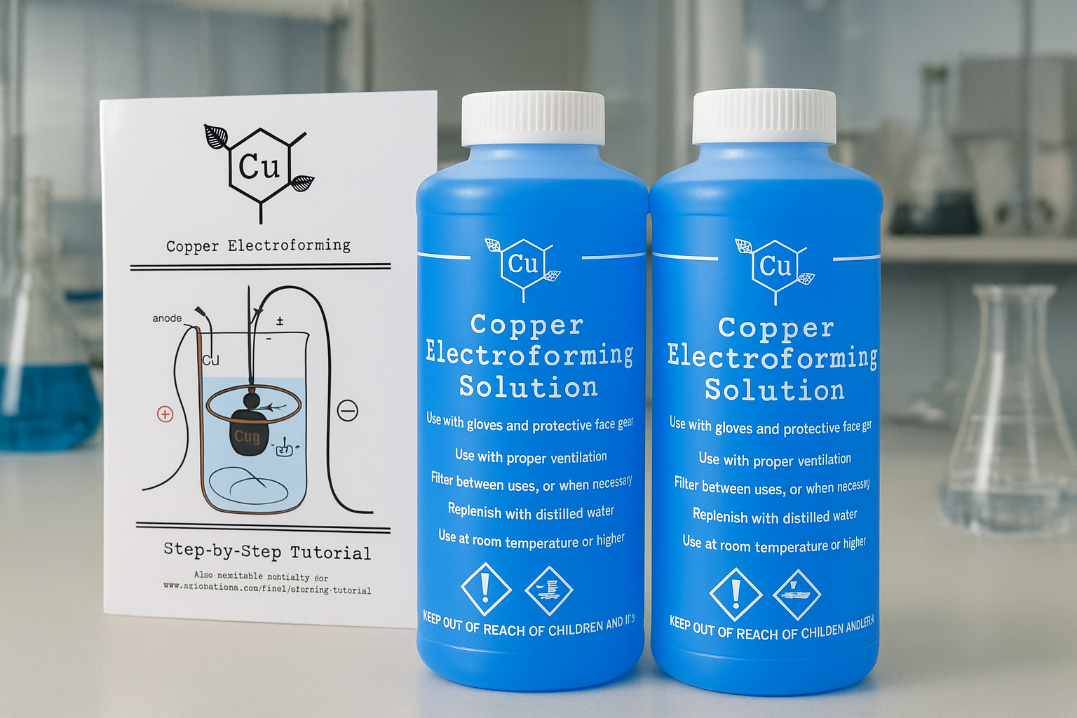
DisChem specializes in providing advanced chemical solutions for lithographic manufacturing. Whether it is hologram production, microlithography, or electron beam lithography, DisChem offers tailored products that improve efficiency and minimize waste. Our electroforming solution is no exception, ensuring precision and quality in every application. Optimized Electroforming Solutions for High Purity Results DisChem’s electroforming solutions deliver electronic-grade […]

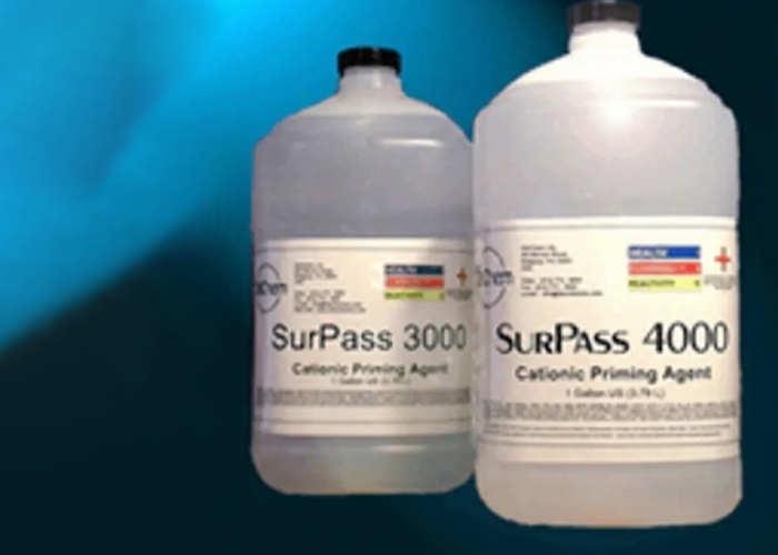
When precision matters in advanced lithography, Lithography Resist Adhesion becomes a critical factor for successful manufacturing. DisChem stands out by offering specialized chemical solutions tailored for micro and nano-fabrication processes. From hologram production to cutting-edge microlithography, DisChem’s products address adhesion challenges while improving efficiency and reducing waste. SurPass Chemical Co Inc and Superior Adhesion SurPass […]

Are you looking for effective electroforming solutions that can enhance your manufacturing processes? Finding the right method can significantly impact the quality and precision of the parts you produce. At DisChem, we focus on providing tailored electroforming services that meet your unique needs. The electroforming process offers a reliable way to create intricate metal parts […]

Are you looking for effective solutions to enhance the quality of your optical discs? The cleaning process is crucial in ensuring that the final product meets high standards. Using the right electroforming cleaners for optical disc applications can significantly impact the performance and durability of your products. At DisChem, we understand the importance of maintaining cleanliness during […]

In the world of semiconductor manufacturing, precision is everything. As we strive for smaller, more complex devices, the materials we use must meet increasingly stringent requirements. Have you considered how critical it is to have access to comprehensive information about your resist materials? The HSQ resist datasheet provides essential insights that can significantly impact your lithography processes […]

Have you ever considered the impact of using a high-quality sulfamate nickel plating solution in your manufacturing processes? The benefits of this specialized plating technique can significantly enhance the performance and longevity of your components. At DisChem, we understand the importance of selecting the right plating solution, and sulfamate nickel plating stands out for its […]

When it comes to semiconductor manufacturing, achieving optimal photoresist adhesion is crucial. Have you ever wondered why some processes yield better results than others? The answer often lies in the application of adhesion promoters, particularly hexamethyldisilazane (HMDS). This chemical plays a vital role in ensuring that photoresists adhere effectively to substrates, which is essential for […]

E-beam lithography is a key tool in creating the tiny patterns needed for modern technology. It uses a beam of electrons to carve precise designs onto materials. This process plays a vital role in fields like electronics, optics, and nanotechnology. At DisChem, we like to simplify complex processes and help explain their value. How E-Beam […]

Charge buildup is a common problem in electron-beam lithography (EBL). If you have dealt with issues like pattern distortion or poor accuracy, you know how frustrating it can be. That’s where DisCharge H2O steps in. This powerful anti-charging agent can help you solve these issues easily. What Is DisCharge H2O? DisCharge H2O, an anti-charging agent, […]

In lithography, having the right products is key. DisChem., Inc. offers adhesion promoters that can make a big difference. At DisChem, we are proud to carry these products. They are designed to improve adhesion on many types of surfaces. What Is SurPass? DisChem specializes in making adhesion promoters for microlithography. Their goal is to help […]

When it comes to electroforming, the choice of solution can make or break the quality of your final product. Are you struggling to find a solution that consistently delivers high precision and meets your specific requirements? At Dischem, we understand that finding the right electroforming solution is crucial for achieving accurate and reliable results. We […]

Are you finding it challenging to secure a reliable partner for your micro lithography projects? Precision in micro lithography is crucial, and even the tiniest error can have significant consequences. So, how can you ensure you’re making the right decision? At DisChem, we understand that your needs are unique, and we tailor our services to […]

Are you looking for a lithography method that offers high precision and flexibility? Direct write electron beam lithography could be the solution you need. This technique allows us to create complex patterns with incredible accuracy, making it ideal for projects that require detailed features on a micro or nanoscale. However, it’s essential to ask the […]

Are you looking for a lithography method that offers high precision and flexibility? Direct write electron beam lithography could be the solution you need. This technique allows us to create complex patterns with incredible accuracy, making it ideal for projects that require detailed features on a micro or nanoscale. However, it’s essential to ask the […]

Are you finding it challenging to secure a reliable partner for your micro lithography projects? Precision in micro lithography is crucial, and even the tiniest error can have significant consequences. So, how can you ensure you’re making the right decision? At DisChem, we understand that your needs are unique, and we tailor our services to […]

When it comes to electroforming, the choice of solution can make or break the quality of your final product. Are you struggling to find a solution that consistently delivers high precision and meets your specific requirements? At Dischem, we understand that finding the right electroforming solution is crucial for achieving accurate and reliable results. We […]

Electron beam lithography (EBL) is a crucial technique in nanofabrication, allowing us to create highly detailed patterns on various substrates. It’s a process that demands precision, and understanding the core issues is essential for achieving the best results. How do we ensure that the patterns are both accurate and reliable? What are the challenges we […]

Don’t you want to know how those incredibly tiny computer chips or intricate electronic components are made? The answer lies in a powerful technique called electron beam lithography (EBL). Think of it as using an incredibly fine pencil to draw on a microscopic canvas. This cutting-edge process allows us to create patterns smaller than the […]

Nickel electroforming is a versatile process used in various industries. By creating precise and durable nickel parts, electroforming has become an essential technique for many applications. Today, we’ll explore what nickel electroforming is, its benefits, and how it can be applied in your work. What is Nickel Electroforming? Nickel electroforming involves depositing a layer of […]

Have you ever wondered how the incredibly complex chips inside your smartphone or computer are made? The answer lies in a process called microlithography. It’s the art of creating tiny patterns on a surface, patterns so small you need a microscope to see them. These patterns form the basis for electronic circuits, optical components, and […]

Have you ever wondered how those incredibly tiny computer chips or intricate microelectronic devices are made? The answer lies in a powerful technique called electron beam lithography (EBL). It’s like having a super-precise drawing tool that can create patterns smaller than the width of a human hair. EBL works by directing a focused beam of […]

Electron beam lithography (EBL) is a powerful technique for creating incredibly tiny features on surfaces. Imagine sculpting circuits thinner than a human hair – that’s the level of precision EBL offers! But this high-resolution magic can be disrupted by a hidden enemy: charge buildup. Here’s where E-beam lithography charge dissipation agents step in, offering a […]

Imagine building intricate circuits smaller than a grain of sand. That’s the magic of microlithography, a powerful technique for etching microscopic patterns onto surfaces. But achieving such precision requires a strong foundation. Here’s where microlithography adhesion promoters come in, offering a solution to a critical challenge: ensuring the resist sticks firmly to the substrate during […]

When it comes to precision in microfabrication, the materials you choose can make all the difference. One standout material is hydrogen silesquioxane EBL negative resist. This article delves into why this resist is crucial for anyone involved in electron beam lithography (EBL). Understanding Hydrogen Silesquioxane EBL Negative Resist Hydrogen silesquioxane (HSQ) EBL negative resist is […]

Electron beam lithography (EBL) is a powerful technique for creating incredibly tiny features on surfaces. Imagine sculpting circuits thinner than a human hair – that’s the kind of precision EBL offers! But this high-resolution magic comes with a learning curve. E-beam lithography systems can seem complex, and choosing the right one can feel overwhelming. So, […]