Why E-Beam Lithography Systems Matter in AI Chip Manufacturing?
Jun 12, 2026
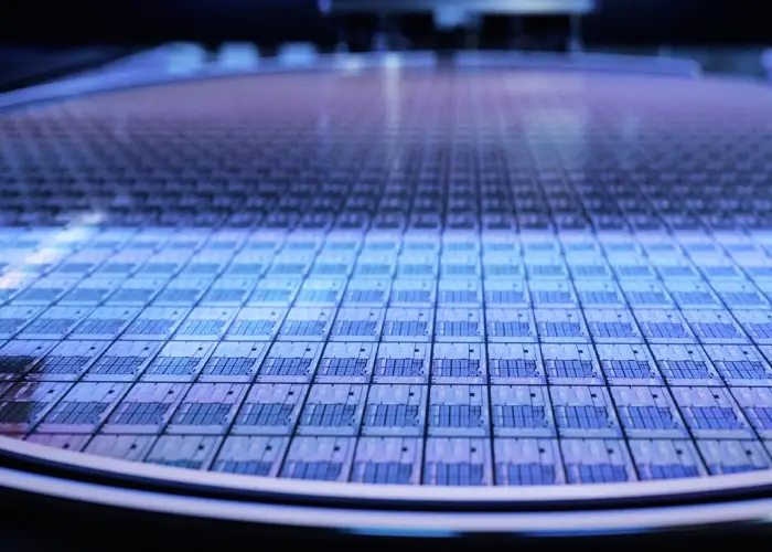
In modern microfabrication, working at the nanometer scale means that even the smallest variation can define the success or failure of a device. Engineers in semiconductors, MEMS, and photonics operate in a domain where precision is paramount, and minor deviations can have cascading consequences.
Substrate inconsistencies resist adhesion failures, and subtle differences in exposure conditions can disrupt entire fabrication processes. In such a delicate environment, (EBL) Electron Beam Lithography has become an essential tool, enabling engineers to achieve the accuracy required for groundbreaking work. However, technology alone is not enough; achieving consistent results requires high-quality materials and expert guidance at every step.
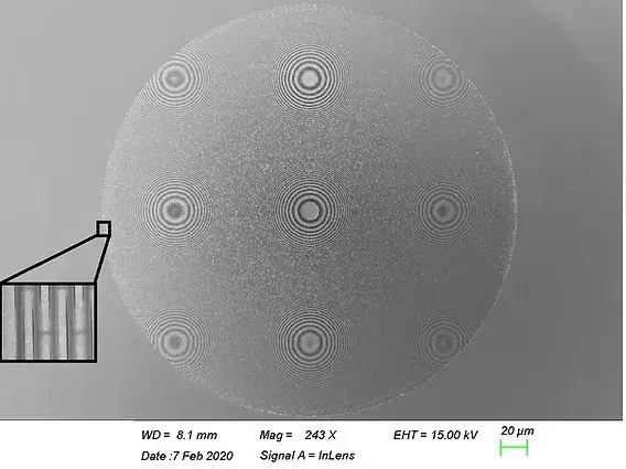
Despite advanced equipment, nanoscale fabrication presents several hidden challenges that can compromise results. Resist adhesion issues can lead to peeling and defective patterns, while substrate charging can distort even the most meticulously designed features.
Minor variations in line edges or surface uniformity may seem insignificant, but they can affect the electrical performance and reliability of devices. In high-stakes applications where timing and precision matter, such challenges can increase production costs, extend timelines, and force repeated iterations, ultimately slowing innovation and diminishing efficiency. Traditional lithography techniques often struggle to address these challenges, which is why engineers are turning to direct-write solutions like EBL Electron Beam Lithography.
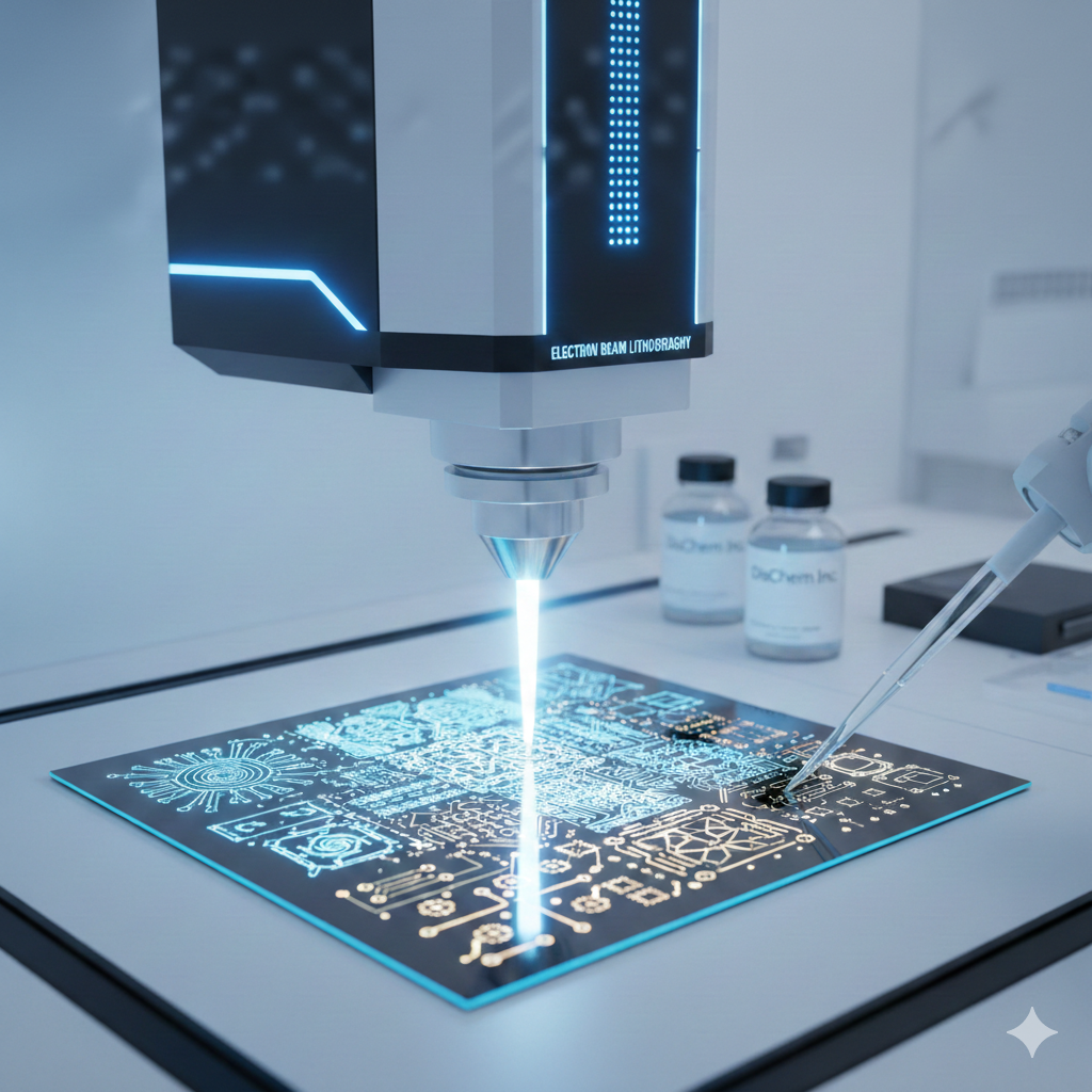
Electron Beam Lithography provides engineers with the ability to write patterns directly onto substrates, eliminating the limitations of mask-based approaches. This direct-write capability allows for remarkable control over sub-10-nanometer features, enabling the creation of intricate designs with unprecedented accuracy.
Engineers can iterate designs rapidly without the need for multiple masks, ensuring that modifications are implemented immediately and precisely. The result is not just faster prototyping, but also reduced material waste and lower defect rates. By integrating EBL into their workflows, teams gain the freedom to experiment with complex patterns and structures, pushing the boundaries of innovation while maintaining consistent quality.
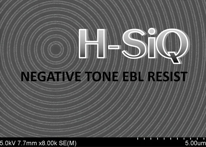
Achieving reliable results with Electron Beam Lithography is not only about the technology; it also depends on the quality of the materials and support behind it. DisChem Inc. provides high-purity electron-beam resists and specialized substrate preparation solutions designed to minimize charging and improve adhesion. Alongside their products, DisChem Inc. offers expert guidance on exposure, resist selection, and development processes, ensuring that every step of the fabrication workflow is optimized. By addressing both materials and procedural challenges, DisChem Inc. helps engineers achieve consistent results, reduce defects, and accelerate innovation, making them more than a supplier they are a partner in precision microfabrication.
Integrating Electron Beam Lithography into a microfabrication workflow can be complex, but with the right materials and expertise, engineers can achieve highly predictable results. Uniform resist application and carefully controlled exposure parameters help maintain the integrity of patterns, while precise substrate preparation reduces the risks associated with charging and adhesion problems.
These factors combine to minimize variability and defects, allowing engineers to dedicate more time to innovation rather than troubleshooting. With streamlined workflows, teams can iterate designs faster, produce cleaner nanoscale features, and maintain consistent performance across multiple fabrication runs.
As device geometries continue to shrink and designs become increasingly complex, traditional lithography methods struggle to keep pace. Electron Beam Lithography offers the flexibility engineers need to meet these evolving demands.
It enables rapid prototyping of advanced semiconductor devices, fabrication of high-density MEMS arrays, and development of intricate photonic circuits, all with remarkable precision. When paired with DisChem Inc.’s high-quality materials and technical guidance, EBL becomes a future-proof solution, allowing engineers to scale from experimental prototypes to production without sacrificing consistency or quality.
The benefits of using (EBL) Electron Beam Lithography extend beyond technical precision. By reducing defects and rework, engineers experience higher yields and more predictable outcomes. Faster iteration cycles allow teams to explore more ambitious designs, testing new concepts without fear of wasted materials.
The increased confidence in reproducibility and reliability empowers engineers to innovate freely, transforming complex fabrication challenges into opportunities for discovery. Laboratories and production facilities alike gain a competitive edge by combining EBL with DisChem Inc.’s comprehensive materials and support.
Microfabrication at the nanoscale is unforgiving, and even minor errors can have significant consequences. Electron Beam Lithography, complemented by DisChem Inc.’s solutions, equips engineers with the tools, materials, and expertise to overcome these challenges.
From minimizing defects to enabling rapid design iterations and scalable production, this combination ensures engineers can focus on innovation rather than troubleshooting. For teams working in semiconductors, MEMS, or photonics, EBL with DisChem Inc. is not just a tool it is a necessity for achieving reliable, high-precision microfabrication.
Explore the full range of solutions at DisChem Inc. to experience the precision, reliability, and efficiency that modern microfabrication demands.
Q1: What is EBL Electron Beam Lithography?
A: EBL Electron Beam Lithography is a high-precision microfabrication technique that directly writes nanoscale patterns onto substrates using a focused electron beam, enabling sub-10-nanometer resolution without relying on masks.
Q2: Why is EBL preferred over traditional lithography techniques?
A: Unlike mask-based processes, EBL allows rapid design iteration, higher accuracy, and reduced defects, making it ideal for semiconductor, MEMS, and photonic device fabrication.
Q3: How does DisChem Inc. support EBL processes?
A: DisChem Inc. provides high-purity electron-beam resists, substrate preparation solutions, and expert technical guidance to optimize exposure, adhesion, and reproducibility, ensuring consistent, high-quality results.
Q4: What are common challenges in nanoscale fabrication?
A: Engineers often face resist adhesion failures, substrate charging, and minor line-edge variations, all of which can disrupt pattern accuracy and affect device performance.
Q5: Can EBL be used for both prototyping and production?
A: Yes, EBL offers flexibility to scale from experimental prototypes to full production runs without sacrificing consistency, especially when paired with reliable materials and technical expertise from DisChem Inc.
Call Us Today +1 (814) 772-6603 or email us at info@discheminc.com to book your appointment today.