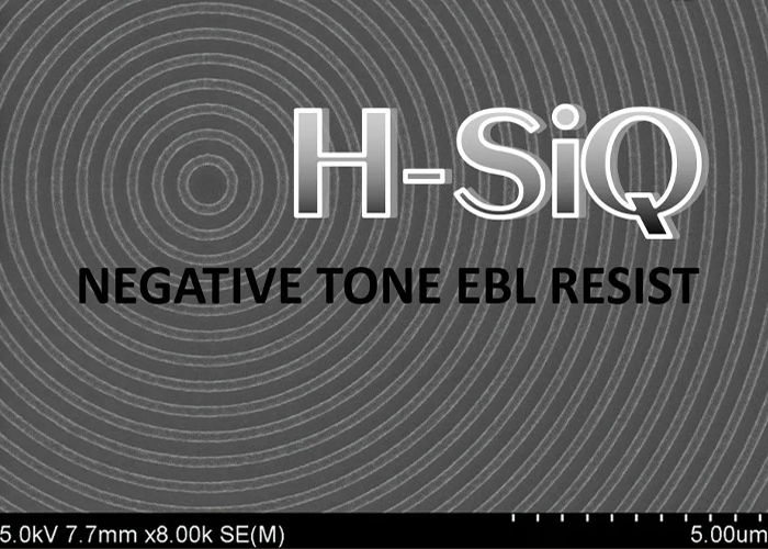
Why HSQ Negative Resist Is the Preferred Choice for High-Resolution Electron Beam Lithography?
Mar 18, 2026
Electron beam charge dissipation is the process of neutralizing or removing built up static electricity from a surface during the making of tiny electronic parts. By providing a path for electricity to flow, this method stops negative particles from gathering and pushing the electron beam off course. Using a reliable electron beam charge dissipation strategy is necessary to reach extreme accuracy, reduce errors, and keep production moving fast in modern computer chip manufacturing.
Table of Contents
1. How an Electron Beam Anti-Charge Agent Saves Time and Money
2. Improving Pattern Accuracy with Electron Beam Charge Dissipation
3. Streamlining Workflows with Modern Electron Beam Charge Dissipation
4. Conclusion
5. Frequently Asked Questions
In the world of high end chip making, accuracy decides your profit. When an electron beam hits a surface that does not conduct electricity, electrons build up. This creates a “charging” effect that pushes the beam away, leading to mistakes in the pattern. Without a dedicated electron beam anti-charge agent, these errors can ruin entire batches of expensive parts. For a business, this means wasted materials and lost hours of expensive lab time.
The main benefit of using a high quality agent like DisCharge is the immediate increase in successful parts. DisCharge is unique because it is a water based solution that does not use a plastic like polymer formula. This special chemistry makes it very stable, giving it a two year shelf life at room temperature. Unlike older agents that must be kept in a refrigerator and filtered to remove tiny clumps, DisCharge does not need to be filtered before you use it. This reliability ensures that your work never stops because of expired or clogged chemicals, saving both time and money.
Beyond stopping static build up, DisChem Inc. provides a variety of specialty cleaners designed to keep your work area perfectly clean. Using these services together ensures that every step of your process from start to finish is set up for the best possible results.
The most important benefit of effective electron beam charge dissipation is the total removal of pattern placement errors. According to research from the SPIE Digital Library, uncontrolled static build up is one of the main causes of defects in small scale printing. When static builds up unevenly, the beam drifts, making it impossible to hit very small targets.
By applying an electron beam anti-charge agent, you create a steady environment. This is vital for:
Using DisCharge provides a steady layer that is very easy to manage. Since the formula is water based, it is safer for the environment and easier for workers to handle compared to harsh chemicals. Because it is stable and does not need filtering, it stays smooth and ensures the electron beam stays focused on its path during the entire process.
Efficiency in a lab depends on how fast you can finish a part from start to finish. Many products used to stop static are hard to remove and require strong chemicals that can damage delicate parts. This adds extra steps to the work and increases the risk of breaking the final product.
DisCharge makes this entire process faster because of its unique formula. Since it is not a polymer agent, it is easily removed with a simple water or alcohol rinse. This easy process protects your tiny structures while cutting down on work time. Also, because it does not need filtering and stays good at room temperature, you spend less time on chemical maintenance and more time on actual work.
In addition to these solutions, DisChem Inc. offers custom chemical mixing services to help labs create special formulas for unique challenges. By using these services, facilities can ensure that all their chemicals work together perfectly to make the job easier.
Effective electron beam charge dissipation is the foundation of successful high tech manufacturing. By using a stable electron beam anti-charge agent like DisCharge, makers can stop costly beam errors and ensure perfect accuracy. DisCharge is a unique, water based formula that stays good for two years at room temperature, does not need filtering, and is easily cleaned off with water or alcohol. These features make it a professional and fast choice for modern manufacturing challenges.
1. What causes static build up in e-beam work?
Static build up happens when the electron beam hits a surface that cannot carry electricity away. The electrons get stuck on the surface, creating an electric field. According to the National Institute of Standards and Technology (NIST), this field pushes the beam away from its target, causing blurry or misplaced patterns.
2. How does an anti-charge agent stop the beam from moving?
An electron beam anti-charge agent adds a very thin layer over the surface that can carry electricity. This layer acts like a small wire, carrying the extra electrons away to a ground point. This keeps the surface neutral so the electron beam can stay perfectly focused on its path.
3. Why is a non-polymer formula better for this work?
Formulas like DisCharge that do not use polymers are more stable. They do not need to be kept in a fridge and they do not grow clumps, which means they do not need to be filtered. This stability allows for a two year shelf life at room temperature, saving labs money on wasted chemicals and storage.
4. Is DisCharge easy to clean off after use?
Yes, DisCharge is made to be cleaned off with just water or alcohol. This is a major benefit because it does not require harsh cleaners that could hurt the tiny patterns you just made. It ensures a clean surface for the next step of the making process without leaving any mess behind.
Call to Action: Protect your results and improve your accuracy today. Contact DisChem Inc. to learn how DisCharge and our other lab chemical services can make your work faster and better.
Brand Positioning: DisChem Inc. is a top provider of high purity chemical solutions. We specialize in innovative products like DisCharge, designed to solve the hardest challenges in electron beam charge dissipation through stable and easy to use chemistry.
Call Us Today +1 (814) 772-6603 or email us at info@discheminc.com to book your appointment today.
Mar 18, 2026
Feb 20, 2026