Why E-Beam Lithography Systems Matter in AI Chip Manufacturing?
Jun 12, 2026

This blog delves into the world of e-beam lithography, exploring its role in transforming nanofabrication. We’ll discuss how e-beam lithography systems offer unprecedented precision and flexibility, enabling the creation of complex nanostructures that are driving innovation in fields like quantum computing and nanophotonics.
Imagine being able to draw intricate patterns on a surface with precision that rivals the finest art. Welcome to the world of e-beam lithography, where technology meets artistry at the nanoscale. This technique is revolutionizing nanofabrication by enabling the creation of complex structures with unprecedented accuracy. But what makes e-beam lithography so special, and how can it transform the future of nanotechnology?
As we explore this technology, we’re not just talking about creating tiny patterns; we’re talking about building the future of computing, medicine, and energy storage. E-beam lithography is at the heart of many cutting-edge innovations, from quantum computing to nanophotonics. So, let’s dive into how e-beam lithography systems are changing the game.
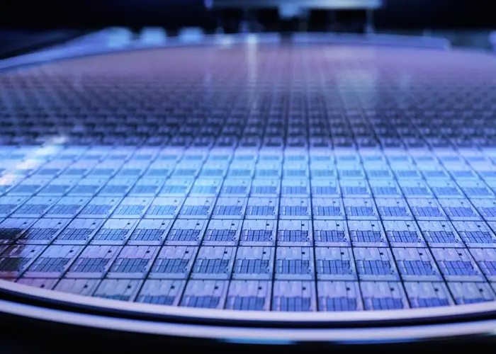
E-beam lithography is like having a super-precise pen for drawing at the nanoscale. It uses a focused beam of electrons to create patterns directly on a substrate, eliminating the need for physical masks. This maskless approach allows for rapid prototyping and flexible design changes, making it a game-changer in nanotechnology research and development.
In the context of an e-beam lithography system, this technology is particularly useful for creating complex patterns that would be difficult or expensive to produce with traditional mask-based methods. For instance, researchers can quickly test new designs without the overhead of fabricating masks, accelerating the development cycle. According to a study by Synopsys, e-beam lithography can achieve sub-10nm resolution with high pattern fidelity, making it ideal for advanced nanofabrication applications (Synopsys, 2020).
This precision is not just theoretical; it’s being used in real-world applications. For example, e-beam lithography is crucial for creating the complex nanostructures needed in quantum computing. By enabling the rapid prototyping of these structures, researchers can explore new possibilities in computing that were previously unimaginable.
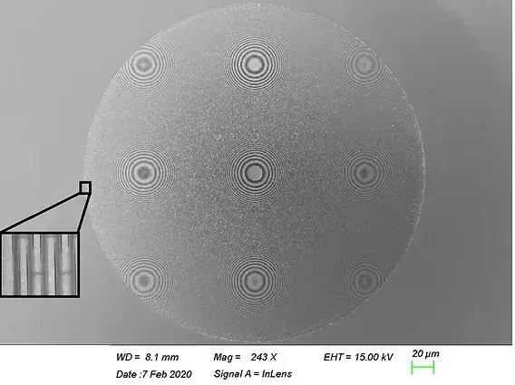
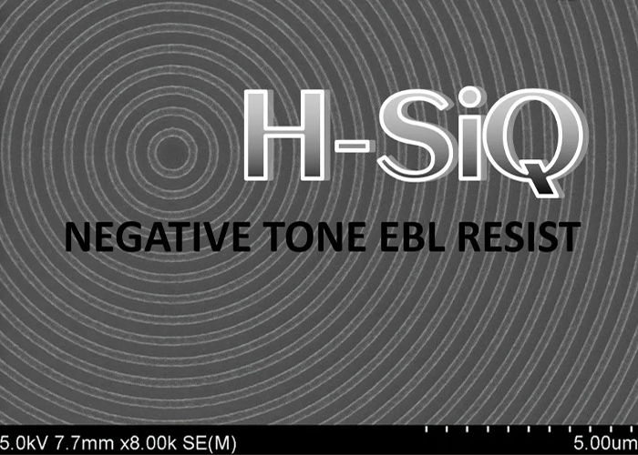
When it comes to e-beam lithography, one of the biggest challenges is charge buildup on insulating substrates. This can lead to pattern distortion and reduced resolution. That’s where EBL anti-charging agents come into play. These agents create a conductive layer that dissipates excess electrons, ensuring accurate pattern formation.
At DisChem, we consider our EBL anti-charging agents to be a crucial component of our e-beam lithography solutions. Our products, like DisCharge H2O, are designed to be safe, effective, and environmentally friendly. By using these agents, manufacturers can significantly improve the reliability and precision of their e-beam lithography processes. This is particularly important for applications where consistency and accuracy are paramount, such as in quantum computing and nanophotonics.
What makes us consider DisChem for these solutions? It’s our commitment to innovation and customer support. We work closely with our clients to ensure that our products meet their specific needs, whether it’s optimizing process conditions or developing new formulations to address emerging challenges.
E-beam lithography is not just for lab experiments; it has real-world applications in fields like quantum computing, nanophotonics, and advanced semiconductor manufacturing. Companies are using e-beam lithography to create prototypes faster and more efficiently than ever before. For example, researchers at MIT have utilized e-beam lithography to develop novel nanostructures for quantum computing applications, showcasing its potential for cutting-edge research (MIT News, 2022).
As we look to the future, e-beam lithography systems will continue to play a vital role in nanofabrication. With ongoing advancements in technology and materials, we can expect even more precise and efficient processes. The integration of e-beam lithography with other nanofabrication techniques will likely lead to new breakthroughs in fields ranging from medicine to energy storage.
For instance, imagine being able to create nanoscale devices that can target specific cells in the body, revolutionizing drug delivery. Or picture batteries that can store energy more efficiently, transforming how we power our homes and vehicles. These are just a few examples of what’s possible with e-beam lithography.
E-beam lithography systems are transforming the landscape of nanofabrication with their precision and flexibility. As we continue to push the boundaries of what’s possible at the nanoscale, technologies like e-beam lithography will remain at the forefront. By leveraging innovations like EBL anti-charging agents from DisChem, manufacturers can ensure that their processes are both reliable and efficient, driving innovation across multiple industries.
So, what does the future hold for e-beam lithography? It’s a future where precision meets possibility, where the boundaries between science fiction and reality continue to blur. As we move forward, it’s clear that e-beam lithography systems will be a key driver of innovation, enabling us to create devices and technologies that were once thought impossible.
Call Us Today +1 (814) 772-6603 or email us at info@discheminc.com to book your appointment today.