Why HSQ Negative Resist Is the Preferred Choice for High-Resolution Electron Beam Lithography?
Mar 18, 2026
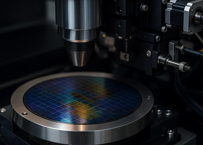
Electron beam lithography plays a vital role in advanced manufacturing environments where ultra-high resolution and precise pattern control are required. It is widely used for applications such as mask writing, nanofabrication, photonics, and exploratory research in next-generation devices. The e-beam lithography system enables feature sizes that extend far beyond the limits of traditional optical lithography, making it indispensable for innovation-driven production. As these processes become more complex, yield optimization increasingly depends on effective charge management during exposure.
Yield is a defining metric for success in any lithographic process, but it carries even greater significance in electron beam lithography due to the serial nature of pattern writing. Each exposure step represents a considerable investment of time and resources. Any process instability that leads to defects or rework can quickly affect throughput, cost efficiency, and production timelines.
As manufacturers push toward tighter tolerances and higher pattern densities, previously minor variations can result in measurable yield loss. Among the many variables that influence process outcomes, surface charging stands out as one of the most persistent challenges affecting yield consistency and pattern accuracy.
Within an e-beam lithography system, a focused electron beam interacts with a resist-coated substrate to define extremely fine features. During this interaction, electrons may accumulate on the surface or within insulating layers when they are not able to dissipate efficiently. This charge build up creates localized electric fields that interfere with the electron beam path.
Even small deviations in beam trajectory can cause placement errors, critical dimension variation, or pattern distortion. These effects become increasingly pronounced as feature sizes shrink and layouts grow more complex. Over time, unmanaged charging contributes to higher defect density and reduced process repeatability.
Effective charge management is fundamental to achieving high yield in electron beam lithography. When charging effects are left unaddressed, engineers may observe inconsistent exposure results that vary across the substrate or between production runs. These inconsistencies often lead to increased inspection failures and downstream processing issues.
Attempts to compensate for charging through exposure parameter adjustments can provide limited relief but often introduce additional complexity into the process. This approach may reduce predictability and extend development cycles. A more reliable strategy focuses on addressing charge accumulation directly at the material and process level.
One of the most effective methods for controlling surface charging is the use of an E Beam Lithography Charge Dissipation Agent. These specialized chemical solutions are designed to enable controlled dissipation of accumulated electrons during exposure. By reducing charge buildup, they help stabilize beam behavior and maintain exposure accuracy.
A properly formulated E Beam Lithography Charge Dissipation Agent supports consistent pattern transfer without interfering with resist sensitivity or resolution. This improves feature uniformity, minimizes line edge variation, and enhances overall process reliability. These benefits directly translate into improved yield and reduced defect rates.
At DisChem Inc., charge dissipation solutions are developed with a deep understanding of advanced lithographic environments. The focus is on creating chemistry that performs reliably under real-world manufacturing conditions while integrating smoothly into existing workflows.
Modern e beam lithography systems operate within tightly controlled process windows that demand high material compatibility. Any additional chemistry introduced into the process must work seamlessly with existing resists, substrates, and exposure parameters.
DisChem Inc. designs its chemical solutions to align with these requirements. Charge dissipation agents are engineered to complement tool performance rather than complicate it. This allows manufacturers to improve charge control without sacrificing throughput, flexibility, or process simplicity.
By improving stability at the substrate level, manufacturers can achieve more predictable exposure results across varying pattern densities and design complexities. This consistency is essential in both research environments and production settings where multiple applications may share the same equipment.
Stable processes are the foundation of long-term yield improvement. When charging effects are minimized, engineers can rely on consistent beam behaviour rather than adjusting parameters to compensate for unpredictable variation. This simplifies process optimization and accelerates the transition from development to production.
Improved charge control also enhances repeatability across batches and substrates. This is especially important for applications that demand high reliability and tight dimensional control. By reducing exposure variability, effective charge management supports robust manufacturing outcomes.
DisChem Inc. supports these goals through continuous innovation in lithographic chemistry. By focusing on real process challenges, the company helps manufacturers achieve dependable performance in increasingly demanding electron beam applications.
Higher yield directly contributes to lower manufacturing costs. When defects are reduced, fewer substrates are scrapped and less material is consumed. Improved first-pass success rates also reduce tool time spent on rework, increasing overall productivity.
Addressing charging at the chemical level allows manufacturers to avoid overly complex compensatory process adjustments. This leads to simpler workflows and more efficient use of resources. These improvements align with DisChem Inc.’s commitment to reducing cost and process waste across advanced lithographic manufacturing.
From holography and optical media to state-of-the-art microlithography and electron beam processes, DisChem Inc. provides solutions that support both performance and sustainability.
As electron beam lithography continues to advance, the importance of effective charge management will only increase. Yield, process stability, and cost efficiency are all closely linked to how well charging effects are controlled during exposure. Left unmanaged, surface charging can undermine even the most sophisticated e beam lithography system.
Through the use of an advanced E Beam Lithography Charge Dissipation Agent, manufacturers can address one of the most critical factors influencing yield. By stabilizing beam behavior and improving pattern fidelity, these chemical solutions support consistent, high-quality results across complex applications.
DisChem Inc. remains dedicated to enabling progress in advanced lithographic manufacturing. By combining deep process knowledge with innovative chemical solutions, the company helps manufacturers improve yield, reduce waste, and confidently push the boundaries of electron beam lithography.
Charge management is critical because surface charging can deflect the electron beam, distort patterns, and reduce dimensional accuracy. Without proper charge control, even advanced electron beam lithography processes can experience lower yield, increased defects, and reduced process repeatability.
Surface charging occurs when electrons accumulate on insulating or semi-insulating substrates during exposure. In an e beam lithography system, inefficient charge dissipation creates localized electric fields that interfere with beam trajectory, leading to placement errors and pattern distortion.
An E Beam Lithography Charge Dissipation Agent helps neutralize accumulated charge during exposure. By stabilizing beam behavior and minimizing electric field interference, it improves pattern fidelity, reduces defect rates, and supports more consistent yield across complex and high-density designs.
When properly formulated, charge dissipation solutions are designed to work without compromising resist sensitivity or resolution. High-quality agents integrate into existing workflows, supporting accurate exposure while maintaining the fine feature control required in advanced electron beam lithography applications.
Yes, modern charge dissipation agents are developed to be compatible with current e beam lithography systems. They are engineered to function within tight process windows, ensuring seamless integration with existing resists, substrates, and exposure parameters without reducing throughput.
Improved charge control increases first-pass yield and reduces defect-related rework. This lowers material waste, minimizes tool downtime, and improves overall process efficiency. Over time, effective charge management contributes to significant cost savings in advanced lithographic manufacturing environments.
Mar 18, 2026
Feb 20, 2026