Why E-Beam Lithography Systems Matter in AI Chip Manufacturing?
Jun 12, 2026

How do semiconductor manufacturers and researchers achieve nanoscale precision when designing microchips, photonics, and MEMS devices? Traditional lithography methods often hit a resolution limit, but electron beam lithography (EBL) offers a way to push past these barriers. In this Blog, we will explore the electron beam lithography process, its advantages, applications, and key considerations for achieving high-quality results.
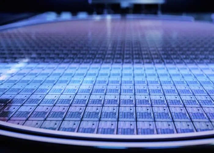
E-beam lithography (EBL) is a cutting-edge, direct-write technology that uses a focused electron beam to pattern resist-coated substrates with sub-10nm precision. Unlike traditional photolithography, which relies on masks and UV light, EBL eliminates the need for masks, enabling faster design iterations and greater flexibility for research and prototyping.
This makes the e-beam lithography process ideal for applications requiring extreme resolution and intricate nanostructures, such as semiconductor fabrication, photonics, and MEMS (Micro-Electro-Mechanical Systems). By offering unparalleled control over patterning, EBL has become indispensable in industries pushing the boundaries of nanotechnology.
The e-beam lithography process involves three critical steps:
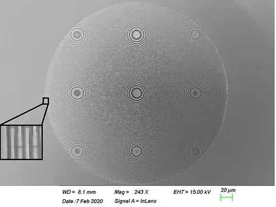
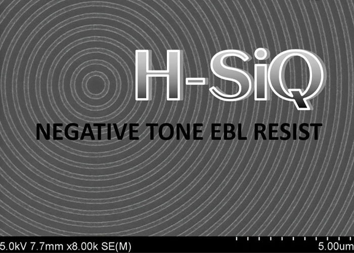
A substrate (silicon, glass, or compound semiconductors) is coated with an electron-sensitive resist like HSQ or PMMA.
High-purity resists ensure better resolution and pattern fidelity.
A focused electron beam scans the resist, altering its solubility in specific areas based on the design pattern.
Exposure settings determine resolution, feature size, and line edge roughness.
The exposed resist undergoes development to reveal the desired pattern.
High-performance developers ensure sharp patterns with minimal defects before etching or deposition onto the substrate.
Using high-quality materials like DisChem’s HSQ resists and developers ensures optimal results in each step of the process.
E-beam lithography offers several advantages over traditional lithographic techniques:
Extreme Resolution: Capable of creating patterns below 5nm for advanced nanofabrication.
Maskless Process: Eliminates mask production costs, enabling rapid design changes during prototyping.
Customizable Exposure: Allows for intricate designs with high complexity and precision.
Broad Material Compatibility: Works seamlessly with silicon, glass, compound semiconductors, and more.
However, achieving these benefits depends heavily on using high-purity materials like HSQ resists and specialized developers—areas where DisChem excels.
E-beam lithography is widely used across industries driving technological innovation:
Semiconductor Fabrication: Enables next-generation nanoelectronics with sub-10nm transistors.
Photonics & Optoelectronics: Creates waveguides, quantum dots, and other optical components.
MEMS & NEMS: Manufactures precision sensors and microstructures for automotive or medical devices.
Quantum Computing & Research: Patterns high-performance qubits and superconducting circuits essential for quantum devices.
These applications highlight how critical precise patterning is to advancing technologies in diverse sectors.
At DisChem Inc., we understand that achieving nanoscale precision requires premium materials designed specifically for e-beam lithography processes. That’s why we offer:
HSQ Resists (Hydrogen Silsesquioxane): Industry-leading negative-tone resists known for ultra-high resolution and exceptional etch resistance.
E-Beam Developers: Engineered to deliver sharp patterns with minimal defects.
Specialized Lithographic Chemicals: Ensures consistency, reliability, and high performance throughout your fabrication process.
Manufacturers and researchers trust us because we prioritize quality and innovation in everything we do:
High Purity & Consistency: Our materials are rigorously tested to meet the highest industry standards.
Expert Support: Our team works closely with clients to optimize processes and troubleshoot challenges.
Reliable Supply Chain: We ensure timely delivery so your projects stay on track without delays.
By choosing DisChem Inc., you’re not just buying materials—you’re partnering with a company committed to advancing your nanofabrication goals.
E-beam lithography is revolutionizing nanofabrication by offering unmatched precision and flexibility across industries like semiconductors, photonics, MEMS/NEMS manufacturing, and quantum computing. However, achieving optimal results depends on using high-quality materials tailored to meet the demands of this sophisticated process.
At DisChem Inc., we provide premium HSQ resists, advanced developers, and expert support to help you achieve superior results in your e-beam lithography projects. Whether you’re a researcher exploring new frontiers or a manufacturer scaling up production, our solutions are designed to meet your needs at every step of the process.
Call Us Today +1 (814) 772-6603 or email us at info@discheminc.com to book your appointment today.