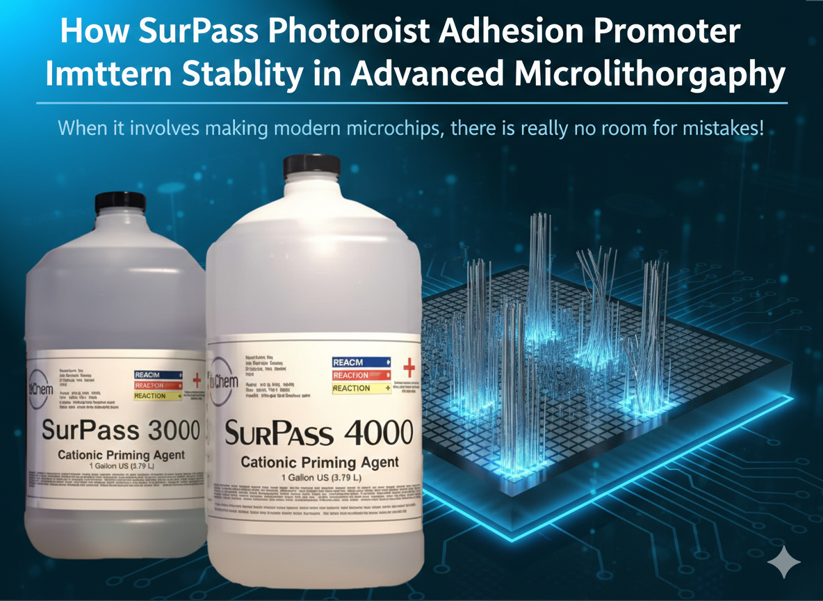
How SurPass Photoresist Adhesion Promoter Improves Pattern Stability in Advanced Microlithography
Feb 20, 2026
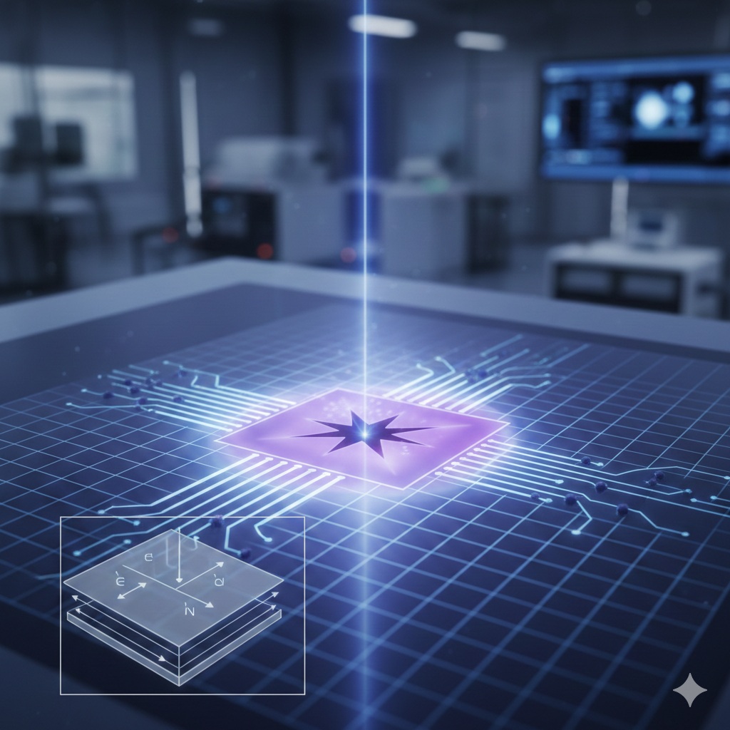
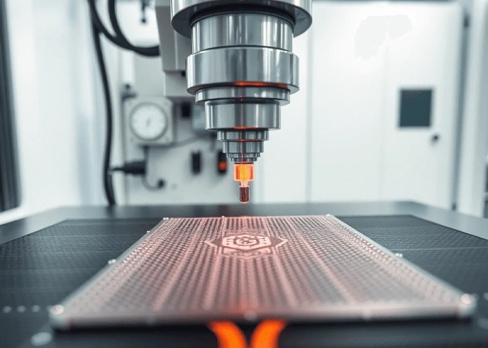
High-resolution electron beam lithography is a cornerstone of advanced manufacturing technologies, supporting applications that range from holograms and optical media to microlithography and next-generation nanofabrication. As feature sizes shrink and pattern complexity increases, controlling defects becomes increasingly challenging. One of the most common and disruptive sources of defects in these environments is surface charging. Effective electron beam charge dissipation plays a vital role in minimizing these issues and maintaining consistent, high-quality results.
DisChem provides innovative chemical solutions designed to meet the demands of advanced lithographic manufacturing. By focusing on yield improvement, cost reduction, and process efficiency, DisChem supports manufacturers who rely on precision and repeatability. Understanding how electron beam charge dissipation works and how an electron beam anti-charge agent supports this process is essential for achieving defect reduction in high-resolution e-beam workflows.
Surface charging occurs when electrons delivered by the beam accumulate on resist layers or substrate surfaces that do not conduct charge efficiently. Many materials used in e-beam lithography are insulating or semi-insulating by nature. As exposure progresses, trapped electrons create localized electric fields that alter the path of the incoming beam.
These unintended electric fields can deflect the electron beam, leading to misplaced features, line width variations, and distorted patterns. In high-resolution processes where tolerances are extremely tight, even minimal charging can result in significant defects. Without proper electron beam charge dissipation, manufacturers may struggle to achieve consistent outcomes across substrates and production runs.
Electron beam charge dissipation helps neutralize excess electrons before they interfere with beam accuracy. By allowing charge to disperse evenly, the exposure environment remains stable and predictable. This stability is essential for preserving pattern fidelity, especially in dense or complex layouts.
When charge dissipation is effective, the electron beam maintains its intended trajectory. Features are written where they are designed, edges remain sharp, and dimensional accuracy is preserved. This level of control is critical for applications that depend on nanoscale precision and repeatable performance.
Inadequate control of surface charging can introduce a range of defects that directly impact yield. These defects include pattern displacement, uneven line widths, feature merging, and stitching errors in large or complex designs. Over time, these issues can lead to higher rejection rates and increased rework.
Poor charge control also affects process repeatability. Variations in charging behavior between substrates or batches can make it difficult to maintain consistent quality. This unpredictability increases production costs and limits scalability. Electron beam charge dissipation addresses these challenges by creating a more uniform electrical environment during exposure.
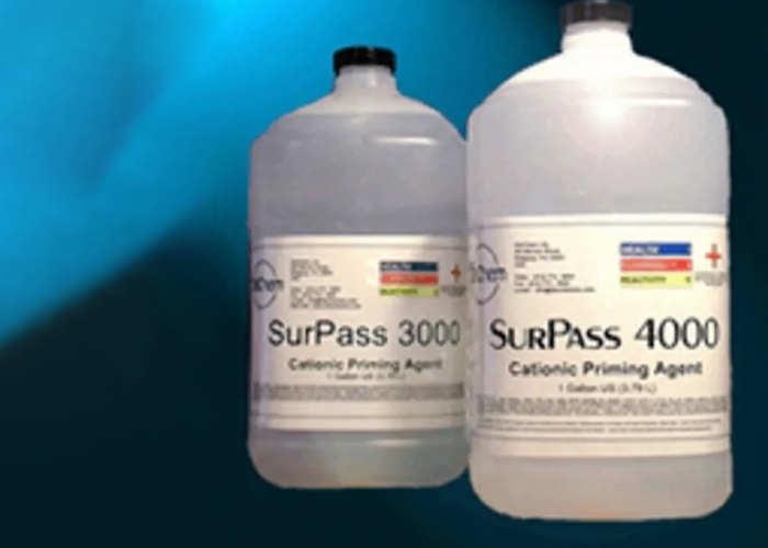
An electron beam anti-charge agent is formulated to reduce surface charging by providing a conductive pathway for excess electrons. Applied as a thin layer, it helps prevent charge buildup without interfering with resist performance or pattern development.
DisChem develops electron beam anti-charge agent solutions that are compatible with advanced lithography materials and workflows. These solutions are designed to integrate smoothly into existing processes, helping manufacturers achieve stable exposure conditions without introducing unnecessary complexity.
By supporting efficient electron beam charge dissipation, an anti-charge agent reduces beam deflection and enhances overall process control. This results in fewer defects and more reliable patterning outcomes.
Exposure stability is a key factor in defect reduction. When surface charging is minimized, the electron beam interacts with the resist in a controlled and uniform manner. This consistency reduces variations in dose delivery and feature placement.
With proper electron beam charge dissipation, manufacturers experience fewer pattern distortions and improved critical dimension control. These improvements are particularly valuable in high-resolution applications where minor deviations can compromise device performance or optical functionality.
Yield improvement is one of the most significant benefits of effective charge dissipation. By reducing defect rates, manufacturers can increase the number of usable devices per substrate. This improvement directly impacts production efficiency and overall cost effectiveness.
An electron beam anti-charge agent also reduces the need for corrective processing steps such as re-exposure or redesign. Fewer process interruptions mean faster throughput and more predictable production schedules. Over time, these efficiencies contribute to reduced material waste and lower operational costs.
Modern e beam lithography supports a wide range of materials and increasingly complex designs. Charge dissipation solutions must be adaptable enough to perform reliably across these varied environments. DisChem focuses on developing chemical solutions that support both current and emerging applications.
Effective electron beam charge dissipation allows manufacturers to work with challenging substrates and high aspect ratio structures without sacrificing precision. This flexibility is essential for research and production environments where innovation and adaptability are critical.
Ease of integration is an important consideration for any process enhancement. DisChem electron beam anti-charge agent solutions are designed to fit seamlessly into established workflows. They can be applied using standard techniques and do not require extensive changes to equipment or procedures.
This straightforward integration allows manufacturers to adopt improved electron beam charge dissipation practices without disrupting production. As a result, teams can achieve better results while maintaining operational continuity and efficiency.
DisChem brings deep expertise in chemical formulation and advanced lithographic processes. Rather than offering generic products, DisChem works closely with customers to understand their specific challenges and performance goals. This collaborative approach ensures that electron beam charge dissipation solutions are practical, effective, and aligned with real world manufacturing needs.
By prioritizing yield improvement and process reliability, DisChem helps manufacturers achieve consistent results in demanding high-resolution e-beam environments. This focus on performance and partnership sets DisChem apart as a trusted provider of advanced chemical solutions.
Flawless performance in high-resolution e-beam lithography depends heavily on effective management of surface charging. Electron beam charge dissipation plays a critical role in reducing defects, preserving pattern fidelity, and maintaining process stability across complex and demanding applications. When surface charge is controlled, manufacturers achieve sharper features, improved dimensional accuracy, and more predictable outcomes.
By incorporating a well-designed electron beam anti-charge agent, manufacturers can significantly minimize beam deflection, reduce rework, and improve overall yield. DisChem supports these goals through innovative chemical solutions developed specifically for advanced lithographic manufacturing. With deep technical expertise and a commitment to collaboration, DisChem helps engineers transform high-resolution e beam processes into reliable, efficient, and scalable production workflows that drive innovation while reducing cost and process waste.
FAQs