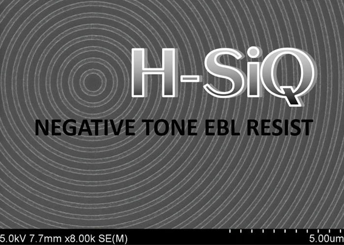
Why HSQ Negative Resist Is the Preferred Choice for High-Resolution Electron Beam Lithography?
Mar 18, 2026

Manufacturers and R&D labs face high stakes with microfabrication. Yield, speed, and design flexibility impact everything from quantum chips to advanced photonics. As devices shrink and pattern fidelity tightens, does your patterning technology truly keep up? Here we review why an E beam lithography system is more than a niche tool, and why it may reshape how pioneering teams approach custom fabrication and demanding prototyping.
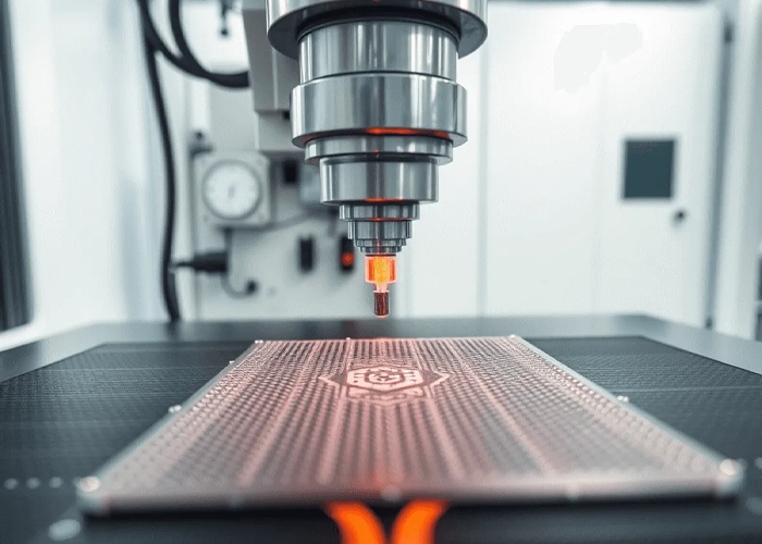
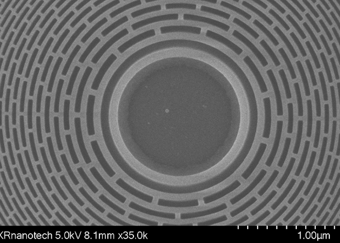
Let’s get right to the point: Today’s advanced designs demand more than traditional mask-based processes can deliver. The E beam lithography system takes a maskless, direct-write approach using a focused electron beam to “draw” features at the nanoscale. The payoff? Sub-10 nm patterning that enables quantum devices, next-gen semiconductors, and advanced photonic components , all with rapid iteration and design flexibility. Our clients tell us this direct-write capability slashes development delays and design risk when pushing into new territory.
With product cycles accelerating, change is always around the corner. Unlike photolithography, E beam lithography lets us update patterns on-the-fly without costly and time-consuming mask fabrication. Flexible design means rapid prototyping, one-off runs, and updates for evolving specs become practical realities. That’s priceless for R&D environments and small-batch innovation, but also for scaling new concepts to production without major delays.
Precision is the name of the game. Modern E beam lithography systems combine advanced beam control, environmental isolation, and automated software. This synergy minimizes errors from external noise, keeps stage motion precise, and ensures repeatable results, even for the most demanding patterns. Environmental stabilization and state-of-the-art vector scan technology deliver that coveted blend of accuracy and reliability for high-resolution projects.
Every technology brings its challenges, and E beam lithography is no different. Throughput is traditionally lower than optical processes, reflecting the serial exposure required for each design. That’s why we collaborate with our partners to manage expectations, optimize settings, and unlock new efficiencies. For those new to the technology, careful workflow management and tailored recipes help bridge the gap between scientific power and practical output.
At DisChem Inc., we see E beam lithography as more than a tool, it’s a strategic advantage. We not only provide the equipment, but also partner with you step-by-step, from process development to troubleshooting. Our team offers expert insights, chemistry solutions (think anti-charging agents), and hands-on integration to make nano-precision a daily standard, not an exception. We’re invested in making sure E beam lithography supports your growth, innovation, and business goals directly.
Would elevating your microfabrication capability help you leapfrog the competition? Are you curious about how E beam lithography can fit right into your production or research strategy? Let’s talk about your needs, timeline, and target outcomes.Phone: +1 (814) 772-6603 | Email: jsmith@discheminc.com
Mar 18, 2026
Feb 20, 2026