Why HSQ Negative Resist Is the Preferred Choice for High-Resolution Electron Beam Lithography?
Mar 18, 2026

Electron beam nanolithography is reshaping how industries approach nanoscale design. For businesses operating in high-stakes sectors like semiconductors, medical devices, and quantum computing, it’s no longer just about reducing feature sizes — it’s about improving repeatability, precision, and scalability. As capital-intensive sectors aim to optimize every dollar invested in R&D and production, the need for more deterministic, high-resolution patterning is undeniable.
At DisChem Inc., we have observed a growing shift in how organizations evaluate lithography tools. While traditional photolithography still dominates for volume production, more businesses are leveraging electron beam techniques where critical dimension control is non-negotiable. So, how does this technology stack up for leaders making strategic decisions?
Table of Contents
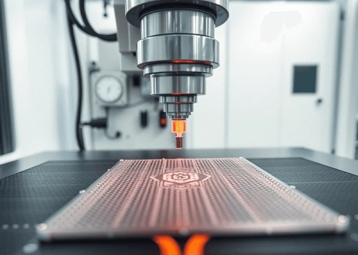
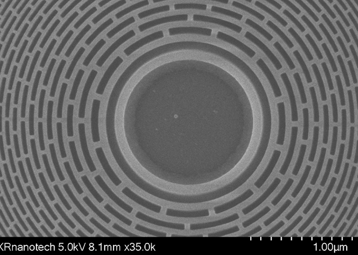
Electron beam lithography (EBL) achieves sub-10 nm resolution, unmatched by even the most advanced deep ultraviolet (DUV) lithography systems. It relies on a focused beam of electrons to write custom patterns directly onto a resist-coated substrate. Unlike mask-based photolithography, the electron beam writes point-by-point, allowing for extreme accuracy and customization.
This method is particularly valuable in research and development environments, where quick iteration cycles and ultra-fine patterning are necessary. Companies developing quantum devices, MEMS sensors, or next-gen photonics rely on EBL for early-stage prototyping. It’s less about scale and more about certainty.
Let’s consider where EBL has clear strategic value:
● Custom Microdevices: Ideal for fabricating microfluidic chips, MEMS sensors, or photonic crystal structures.
● Quantum and Cryogenic Electronics: Where electron tunneling junctions need repeatable nanoscale accuracy.
● Small-Batch Prototyping: Avoids costly mask creation for quick test runs.
A 2024 study published by the IEEE Nanotechnology Council reported that startups using EBL for prototyping shortened product development timelines by up to 30%.
That said, we know this isn’t an all-or-nothing decision. For volume manufacturing, optical systems still lead. But where the cost of errors is high, EBL holds the edge.
Yes, EBL is slower. But let’s not conflate throughput with profitability across all use cases. For high-mix, low-volume production — common in aerospace sensors, prototype chips, and medical diagnostics — EBL actually reduces total cost of ownership (TCO).
Recent data suggests that using EBL in early prototyping can reduce R&D cycle time by up to 28%. That translates to faster time-to-market, which is often more critical than throughput in capital-intensive innovation environments.
Moreover, equipment from advanced vendors now supports multi-beam systems and pattern stitching, helping close the productivity gap without sacrificing accuracy.
We’re seeing strong adoption across industries where accuracy is paramount. EBL’s relevance isn’t theoretical — it’s practical.
For semiconductor clients, it’s increasingly used in developing chiplets and interposers for advanced packaging. The ability to produce high-aspect-ratio features with fewer alignment steps gives EBL an edge over traditional methods.
Not every organization needs EBL — at least not yet. For high-volume manufacturing of memory or logic ICs, the cost-per-wafer and cycle time are still barriers. Furthermore, tool maintenance, electron scattering, and resist sensitivity can introduce complexity in process control.
However, these aren’t dead ends. As EBL systems become more modular and user-friendly, the trade-offs continue to narrow. The technology is evolving from a lab-only tool to a semi-production asset in niche, high-value segments.
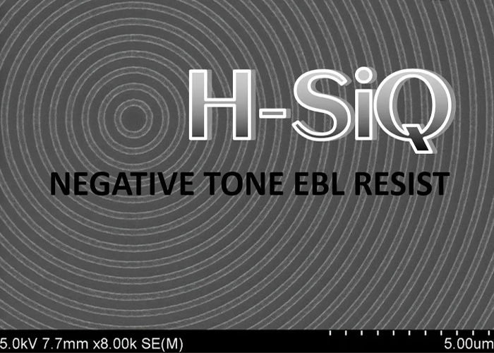
The choice of electron beam nanolithography resist determines not just resolution but also overall pattern fidelity and process reliability.
From our experience and as noted in this resource, we’ve found that:
Depending on your use case — whether you’re targeting lift-off metallization or fine pattern transfer — we often recommend a dual-layer resist stack to balance etch resistance and contrast. Ultimately, aligning the resist type with your business needs can prevent costly downstream defects.
If your business is innovating in areas that require custom nano-patterning — and time-to-accuracy is more important than time-to-volume — then yes, EBL is more than just an R&D tool. It’s a strategic advantage.
That said, our clients at DisChem Inc. don’t just want cutting-edge tech. They want reliability, consistency, and practical ROI. EBL delivers on these fronts when deployed intelligently. As adoption continues to rise in key verticals, it’s time for decision-makers to factor EBL into their digital fabrication roadmap.
So, if you’re evaluating e-beam lithography platforms or exploring custom resist formulations, our specialists are ready to assist. Let’s move precision from lab theory to production reality — together.
Mar 18, 2026
Feb 20, 2026