Why HSQ Negative Resist Is the Preferred Choice for High-Resolution Electron Beam Lithography?
Mar 18, 2026

Curious about how next-generation chips and quantum devices achieve their mind-boggling precision? This blog explores the E-beam lithography process, why it matters for business leaders, and how it’s powering innovation in nanotechnology.
Table of Contents:
Let’s get straight to the point: if you’re leading a company that relies on cutting-edge electronics, photonics, or quantum devices, you already know that traditional manufacturing methods are hitting a wall. The demand for smaller, faster, and more efficient components is relentless. The E-beam lithography process is a game-changer here, offering the kind of nanoscale precision that’s simply out of reach for conventional photolithography.
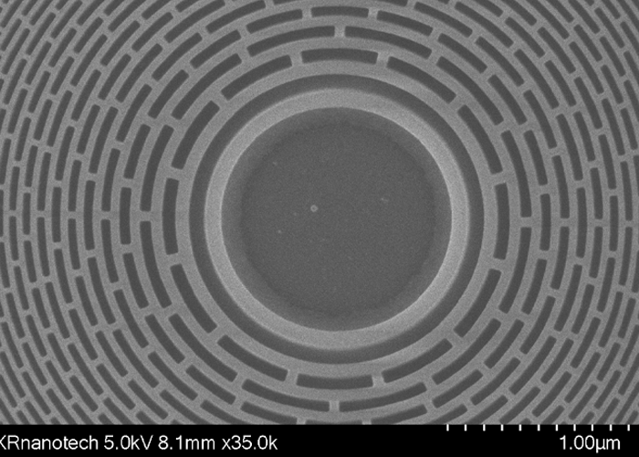
A recent report from NIST highlights that electron beam lithography enables lateral resolutions down to 10 nanometers and placement accuracy of just 1 nanometer. That’s the kind of accuracy that can make or break your next-generation product.
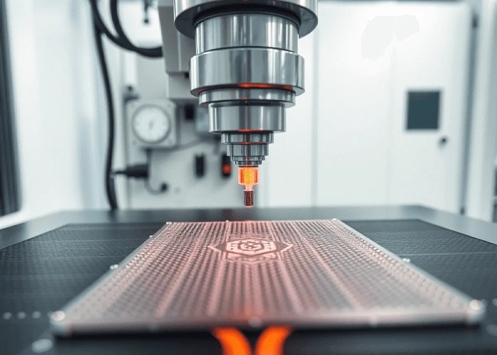
So, what’s the secret sauce? The E-beam lithography process uses a tightly focused electron beam to “write” patterns directly onto a resist-coated substrate. Unlike traditional photolithography, there’s no need for a physical mask. This maskless approach means you can rapidly prototype new designs and iterate without the cost and delay of mask fabrication.
The process goes like this:
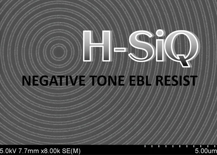
With this method, we’re talking about feature sizes as small as sub-10 nanometers. The flexibility and precision of E-beam lithography make it indispensable for research, prototyping, and specialized manufacturing.
If you’re in R&D, you know how critical rapid iteration is. The E-beam lithography process is a favorite for prototyping because it enables direct writing of new patterns without waiting for custom masks. This means faster time-to-market and more freedom to experiment.
A study from MIT’s RLE demonstrated high-speed E-beam lithography achieving resolutions as fine as nine nanometers, showing its potential for both prototyping and scaling up to mass production.
No technology is without its hurdles. E-beam lithography is slower and more expensive than traditional photolithography for large-scale production. Throughput is limited by the serial nature of the beam, and issues like substrate charging and proximity effects can impact pattern fidelity.
But here’s the good news:
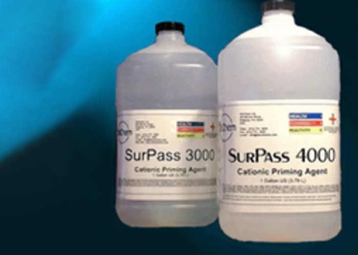
Let’s talk solutions. At DisChem Inc., we know that even the best E-beam lithography process can be derailed by charge buildup on insulating substrates. That’s why we offer anti-charging agents like DisCharge H2O, which forms a thin, conductive layer on top of the resist. This layer dissipates excess electrons during exposure and can be easily removed after processing.
Our approach is simple:
By partnering with us, you get more than chemistry-you get expertise in optimizing every step of your E-beam lithography workflow.
E-beam lithography isn’t standing still. Recent advancements include high-speed multi-beam systems and new resist materials that boost throughput and resolution. The ability to pattern on nonplanar or irregular surfaces is opening doors in flexible electronics and biomedical devices. As more industries push the limits of what’s possible at the nanoscale, E-beam lithography is poised to remain a cornerstone of innovation.
If your business is built on innovation and precision, the E-beam lithography process offers a competitive edge that’s hard to match. Whether you’re prototyping the next quantum device or manufacturing ultra-dense chips, this technology delivers the accuracy and flexibility you need. At DisChem Inc., we’re here to help you overcome the practical challenges and unlock the full potential of E-beam lithography-because when it comes to nanofabrication, every nanometer counts.
Mar 18, 2026
Feb 20, 2026