Why HSQ Negative Resist Is the Preferred Choice for High-Resolution Electron Beam Lithography?
Mar 18, 2026

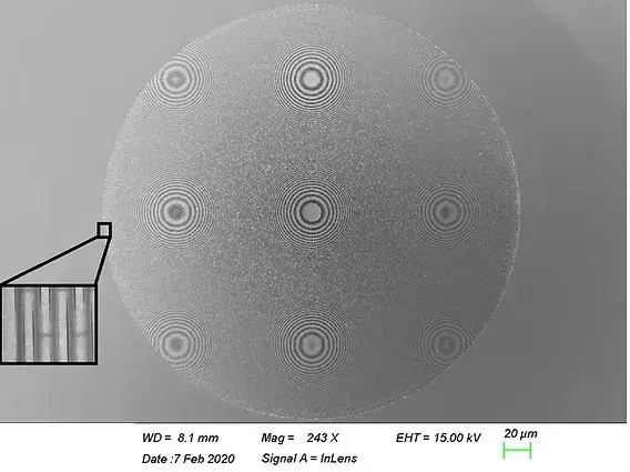
Don’t you want to know how those incredibly tiny computer chips or intricate electronic components are made? The answer lies in a powerful technique called electron beam lithography (EBL). Think of it as using an incredibly fine pencil to draw on a microscopic canvas. This cutting-edge process allows us to create patterns smaller than the width of a human hair, opening up a world of possibilities for technology and innovation.
E-beam lithography involves directing a focused beam of electrons at a surface coated with a light-sensitive material called resist. Where the electron beam hits, it changes the properties of the resist, allowing us to create precise patterns. This process is essential for developing advanced technologies in fields like electronics, semiconductors, and biotechnology.
Table of Contents
ToggleThe e-beam lithography process involves several key steps. First, the substrate is coated with a layer of electron-sensitive resist. Next, the electron beam is used to expose the desired pattern in the resist. The exposed areas of the resist are then developed, removing either the exposed or unexposed parts depending on the resist type. Finally, the remaining resist acts as a mask for etching or depositing the desired material onto the substrate.
E-beam lithography offers unparalleled precision and flexibility compared to other lithography techniques. It allows for the creation of complex and intricate patterns with nanoscale features. However, it can be a time-consuming process, and the cost of equipment can be high.
While e-beam lithography is a powerful tool, it’s not without its challenges. One of the primary concerns is the high cost of equipment and the relatively slow throughput compared to other lithography methods. Additionally, factors like electron beam scattering and resist sensitivity can affect pattern accuracy.
To address these challenges, researchers and engineers are continually developing new materials, techniques, and software to improve the efficiency and precision of e-beam lithography. Advances in electron optics, resist chemistry, and automation have led to significant improvements in recent years.
At DisChem, we understand the complexities of e-beam lithography. We offer a range of products and services to support your EBL endeavors. From high-performance resists to specialized chemicals, we provide the tools you need to achieve optimal results. Our team of experts can also assist you in selecting the right e-beam lithography system and optimizing your processes.
We believe that by working closely with our customers, we can overcome the challenges of e-beam lithography and unlock its full potential. Contact us today to learn more about our products and services and how we can help you achieve your research and development goals.
E-beam lithography is a critical technology for creating the next generation of devices and materials. While it presents certain challenges, the benefits in terms of precision and flexibility make it an invaluable tool for researchers and engineers. By understanding the e- beam lithography process, selecting the right equipment and materials, and seeking expert support,things will become somewhat easy to handle. This way you can harness the power of e-beam lithography to drive innovation and achieve remarkable results. DisChem is committed to being your partner in this exciting journey.
Call Us Today +1 (814) 772-6603 or email us at info@discheminc.com to book your appointment today.

Mar 18, 2026

Feb 20, 2026
No tags found.
Inquire about our exciting new products and well priced commodities.
Copyright © 2025 DisChem, Inc.. All rights reserved.
