Why HSQ Negative Resist Is the Preferred Choice for High-Resolution Electron Beam Lithography?
Mar 18, 2026

Have you ever wondered how the incredibly complex chips inside your smartphone or computer are made? The answer lies in a process called microlithography. It’s the art of creating tiny patterns on a surface, patterns so small you need a microscope to see them. These patterns form the basis for electronic circuits, optical components, and countless other microdevices that power our modern world.
Microlithography is a multi-step process that involves applying a light-sensitive material called photoresist to a surface, exposing it to light through a mask, and then developing the resist to create the desired pattern. This pattern can then be used as a template for etching or depositing materials, creating the final product.
Table of Contents
ToggleMicro Lithography Inc. is a leading force in the realm of microfabrication, offering cutting-edge solutions that redefine the boundaries of precision engineering. We specialize in crafting advanced technologies that enable the creation of intricate patterns on microscopic scales, forming the bedrock for innovations across industries.
Our expertise encompasses a wide spectrum of microlithography techniques. From the well-established optical lithography to the groundbreaking electron beam lithography and the emerging extreme ultraviolet (EUV) lithography, we possess the knowledge and capabilities to deliver tailored solutions for diverse applications. Whether it’s the production of microchips, biomedical devices, or optical components, our commitment to excellence ensures exceptional results.
We don’t just provide equipment and materials; we offer comprehensive support. Our team of experts works closely with clients to understand their unique challenges and provide tailored solutions. From process optimization to operator training, we are dedicated to empowering our customers to achieve their goals.
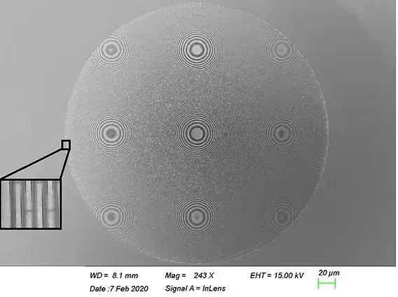
Direct write electron beam lithography (DW-EBL) stands as a pinnacle of precision in the realm of microfabrication. Unlike traditional optical lithography, which relies on masks to transfer patterns, DW-EBL offers unparalleled flexibility and control. It’s akin to an artist wielding a finely tuned brush, meticulously crafting intricate designs at the nanoscale.
This technique involves a focused electron beam that directly writes the desired pattern onto a resist-coated surface. The result is exceptional pattern fidelity and the ability to create highly customized designs. From the development of advanced semiconductors to the fabrication of biomedical devices, direct write- electron beam lithography plays a pivotal role in pushing the boundaries of technological innovation.
However, DW-EBL is not without its challenges. The process can be time-consuming due to the sequential nature of pattern writing. Additionally, achieving optimal results requires careful consideration of factors such as electron beam dose, resist sensitivity, and development conditions.
Microlithography is a cornerstone of modern technology, enabling the creation of the tiny but powerful devices that shape our world. From smartphones to medical implants, microlithography plays a critical role. At DisChem, we are dedicated to pushing the boundaries of this technology and providing our customers with the tools and expertise they need to succeed.
By combining advanced equipment, high-quality materials, and expert support, we empower our customers to achieve their goals in microfabrication. Whether you’re a researcher exploring new frontiers or a manufacturer seeking to optimize your production processes, DisChem is your partner in achieving excellence in microlithography.
Call Us Today +1 (814) 772-6603 or email us at info@discheminc.com to book your appointment today.

Mar 18, 2026

Feb 20, 2026
No tags found.
Inquire about our exciting new products and well priced commodities.
Copyright © 2025 DisChem, Inc.. All rights reserved.
