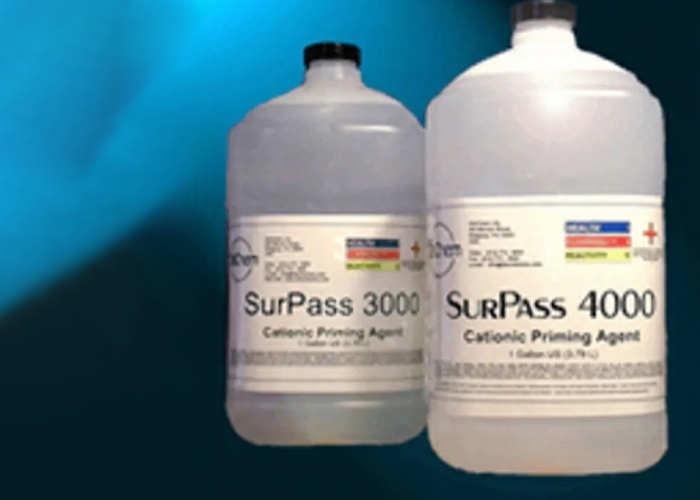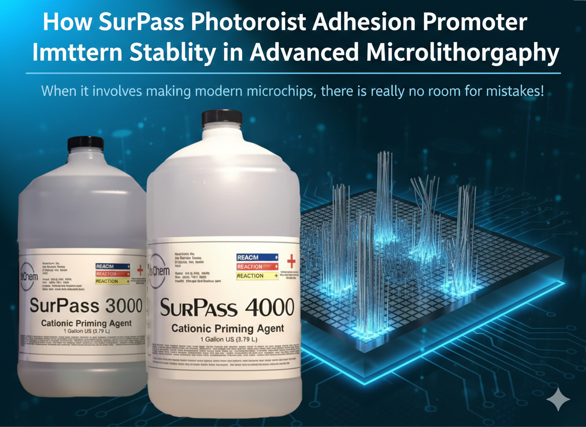
How SurPass Photoresist Adhesion Promoter Improves Pattern Stability in Advanced Microlithography
Feb 20, 2026
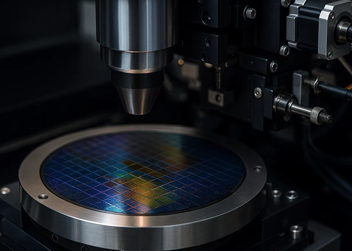
In a laboratory buzzing with the hum of electron-beam systems, engineers hover over microscopes, scrutinizing patterns invisible to the naked eye. Every line, every gap, every edge could make the difference between a device that performs flawlessly and one that fails at scale. This is the world of nanoscale fabrication, a world where precision is not just important; it is everything.
Yet, even the most advanced equipment can’t overcome the unpredictability of materials and processes. Resists that delaminate, substrates that accumulate charge and minor variations in exposure can derail entire projects.
For engineers navigating these challenges, finding reliable solutions is not a convenience; it is survival. That is where Micro Lithography Inc. becomes more than a vendor; it is a partner in problem-solving, helping teams tackle the toughest fabrication challenges with confidence.
In the early stages of microdevice fabrication, small inconsistencies often hide until they manifest as major defects. A line that is not perfectly uniform might disrupt an entire circuit. A resist that does not adhere as expected can peel under the stress of development, forcing engineers to start over. These are not just minor inconveniences they are time-consuming setbacks that waste materials and extend deadlines.
Engineers working with photonic circuits, MEMS, or next-generation semiconductors know this pressure well. The tiniest deviation at the nanoscale can cascade into unpredictable results. And in industries where innovation moves fast, delays can mean missed opportunities.
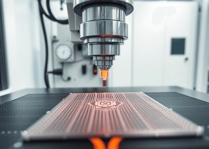
For engineers looking to regain control over this complexity, Direct Write Electron Beam Lithography has become a game-changer. Unlike traditional mask-based processes, direct write EBL allows patterns to be written straight onto the substrate. This means engineers can define intricate features with remarkable accuracy, iterate designs on the fly, and reduce dependency on multiple mask cycles.
With direct write EBL, precision is not just a goal it is a built-in feature. Engineers can produce sub-10-nanometer structures, maintain consistent line edges, and achieve high etch resistance, all while minimizing wasted materials. In practice, this translates to faster prototyping, lower defect rates, and the freedom to explore more ambitious designs without fear of costly errors.
Technology alone does not solve these problems. It’s the combination of high-performance equipment and deep technical expertise that makes the difference. Micro Lithography Inc. provides both, equipping engineers with tools optimized for high-resolution work while offering guidance on workflow, resist selection, and substrate preparation.
This support is crucial. When working at the nanoscale, even small inconsistencies in material behavior or process parameters can produce outsized effects. Micro Lithography Inc’s solutions help engineers stabilize these variables, ensuring reproducible results from one batch to the next. The result is not just reliability, but confidence the ability to innovate without constantly worrying about hidden defects.
Integrating direct write EBL into a production or research environment can feel daunting, but with the right support, the process becomes surprisingly streamlined. Engineers benefit from materials and equipment that have been carefully matched for consistency. Coatings behave predictably. Exposure responses are uniform. Development produces clean, accurate patterns.
By reducing variability, engineers can focus on what matters most: design innovation. Instead of troubleshooting, recalibrating, or compensating for material inconsistencies, teams can spend their time iterating on device performance, testing new concepts, and exploring the limits of what is possible at the nanoscale.
The pace of technology shows no signs of slowing. Device features shrink, complexity grows, and fabrication processes become more demanding. Engineers who rely on Direct Write Electron Beam Lithography and tools from Micro Lithography Inc. are positioned to meet these challenges head-on.
This combination is inherently flexible. Whether it is prototyping a single experimental chip or scaling to a production run of high-density photonic circuits, engineers can trust that their processes remain stable, predictable, and adaptable. A future-proof approach removes uncertainty and allows labs and production facilities to innovate without fear of hitting technical roadblocks.
The impact is tangible. Engineers report cleaner, sharper nanoscale features, fewer defects, and a dramatic reduction in wasted materials. Rework becomes the exception rather than the rule. More importantly, teams can complete projects faster without sacrificing quality, opening the door to more ambitious research and development initiatives.
Precision, repeatability, and confidence these are the results that make Micro Lithography Inc. more than a tool provider. They are a partner in pushing the boundaries of what is possible.
Nanoscale fabrication is unforgiving. Small errors can have large consequences, and traditional methods often fall short. But with the right tools and techniques, engineers can turn complexity into opportunity. Micro Lithography Inc. provides high-performance equipment and technical expertise that ensures reproducible results, while Direct Write Electron Beam Lithography enables the fine control necessary for today’s most demanding designs.
Together, they help engineers overcome persistent challenges, reduce defects, and accelerate innovation. For teams pushing the limits of semiconductors, MEMS, and photonics, this combination is not just a convenience it is a necessity. Explore the full suite of solutions at DisChem Inc. and experience the reliability and precision that modern microfabrication demands.