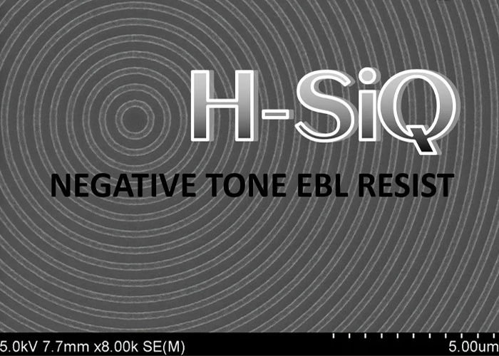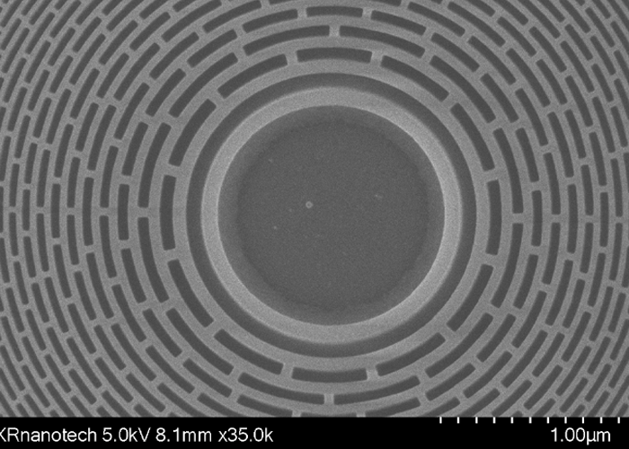
Why HSQ Negative Resist Is the Preferred Choice for High-Resolution Electron Beam Lithography?
Mar 18, 2026

Quick Review
The market for advanced microfabrication is pushing its limits. Every R&D team and innovative manufacturer faces the challenge of creating complex, high-precision structures, sometimes with little room for prototyping. As the push for smaller, faster, and more functional devices continues, direct write electron beam lithography is under a fresh spotlight. Can it offer the flexibility and accuracy needed to support rapid innovation and production scaling?
Table of Contents
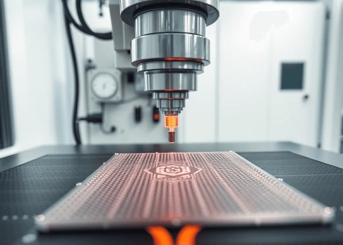
Direct write electron beam lithography is changing the rules for custom patterning at the nanoscale. Unlike traditional methods that require costly and time-consuming photomasks, direct write approaches use a finely focused electron beam to “write” custom designs directly onto a resist-coated substrate. This form of maskless lithography gives our customers the flexibility to create sub-10nm features with precision, making it indispensable for rapid prototyping, device customization, and proof-of-concept fabrication. For organizations where quick turns and true design freedom matter, direct write is often an obvious choice.
Let’s face it: while throughput is still lower when compared to optical methods, direct write electron beam lithography offers unmatched accuracy and geometric versatility. EBL electron beam lithography uses the same direct-writing capabilities, allowing us to go from a digital CAD file straight to a physical prototype. This maskless approach is especially attractive for low-volume, high-mix production and research environments. We see customers benefit from being able to quickly pivot designs and optimize features before committing to scale.
Throughput is a challenge that every electron beam tool vendor has faced for decades. Serial exposure, where each pixel or feature is written one at a time, means larger areas can require significant time investment. But the industry has responded, with developments like massively parallel beamlet arrays, thousands of beams writing in concert, to boost throughput for direct write without sacrificing precision. For DisChem Inc. clients, this means gains in process efficiency and new capabilities that can reduce prototyping turnaround from months to weeks.
No technology comes without trade-offs. Throughput aside, process parameters, like resist sensitivity, beam current, and substrate charging, dictate outcome quality. Issues such as electron scattering or unintended exposure can affect edge roughness in tiny features. But with robust workflow engineering and targeted solutions, like optimized anti-charging agents, tailored resists, or batch-customized write strategies, our team helps customers minimize risk and maximize yield.
One of our clients summed up the advantage: “With DisChem’s guidance, we moved from unpredictable outcomes to consistent, reliable features at sub-20nm, saving both budget and sanity.”
At DisChem Inc., we don’t just provide chemicals. Our hands-on guidance, application know-how, and customized anti-charging formulations have earned us a reputation as a trusted resource for anyone integrating direct write or EBL electron beam lithography workflows. We help clients identify the right tools, engineer application-specific solutions, and provide post-implementation support that keeps projects on track and on pace with their markets. Our approach is collaborative and transparent; we believe modern microfabrication works best as a team effort.
Curious how direct write electron beam lithography could supercharge your next project? Ready to explore solutions that keep you ahead of the competition? Let’s connect, share stories, and map out the best path forward, for today’s application and tomorrow’s ambitions.Phone: +1 (814) 772-6603 | Email: jsmith@discheminc.com
Mar 18, 2026
Feb 20, 2026