Why E-Beam Lithography Systems Matter in AI Chip Manufacturing?
Jun 12, 2026
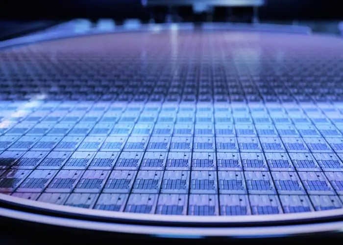
An e beam lithography system is a very important tool for making artificial intelligence (AI) chips. It works like a super-fine pen. It uses a tight beam of electrons to draw tiny lines and patterns directly onto a coated surface. AI chips need billions of tiny switches packed close together to work. This system helps make the master templates and test chips that run modern AI networks. Without this tool, we could not build the tiny brains that smart computers need to think fast.
Using an (ebl) electron beam lithography process to design new chips has clear benefits and challenges that directly affect how we build new technology.
On the good side, this method offers extreme detail. It can draw incredibly tiny lines for complex AI designs. It also offers great flexibility. The machine writes patterns directly from a computer file, so engineers can easily change chip designs without buying expensive stencil plates.
On the bad side, there are drawbacks. The process is quite slow. Drawing patterns point-by-point takes a long time, making it too slow for mass production. Also, the machinery is very expensive to buy upfront.
Even with these drawbacks, we still need this high level of detail to build the master templates that other fast machines copy. This makes the process a vital part of the chip-making pipeline.
Testing a new AI chip can cost a lot of time and money. Choosing your printing method has a massive impact on your project budget.
Old methods use glass stencil plates to print designs. These plates cost millions of dollars and take weeks to make. If you make a single mistake in your design, you have to buy new plates and wait all over again.
Using an (ebl) electron beam lithography process changes this. This tool lets design teams test new ideas immediately. Because the machine writes directly from a computer file, engineers can update their designs in software and print them onto a test chip the very same day. This saves huge amounts of time and cash, helping companies launch new products much faster. Learn more about how this nanoscale writing works on the Wikipedia Electron-Beam Lithography page.
To get the best results from an active e beam lithography system, factories must prevent common mistakes like static electricity buildup.
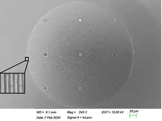
When electrons hit glass or quartz, negative electricity piles up on the surface. This buildup acts like a magnet, pushing away the incoming electron beam. This causes alignment errors and ruins your work, costing your lab a lot of money in lost time and wasted silicon.
To solve this, DisChem created DisCharge H2O, a safe water-based liquid coating. You put it on top of the chip film so the extra electricity flows away safely. This stops the beam from bending and saves factories thousands of dollars in wasted materials, ensuring that your high-tech machines run smoothly without any electrical errors.
You need the right chemicals to get the best results from your e-beam lithography system. Choosing good coatings keeps your success rate high and your waste low.
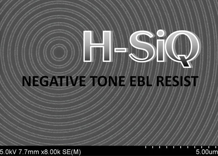
DisChem provides H-SiQ, a high-purity liquid glass resist. When the electron beam hits this chemical, it turns into a durable, silica-like glass. H-SiQ offers superb detail and holds up well against harsh etching gases, ensuring that your tiny designs do not warp or melt during the manufacturing process.
Using reliable, high-performance chemistry improves your success rate, keeps your work on track, and saves money. Read about the chemical details of this compound on the Wikipedia Hydrogen Silsesquioxane page.
Getting your chemical coatings to stick to slippery surfaces like silicon or metals is a major challenge in chip factories.
If the chemical film peels off when you wash it, the tiny lines will fall over and ruin the chip. This issue is called pattern collapse, and it is a leading cause of broken chips in research labs.
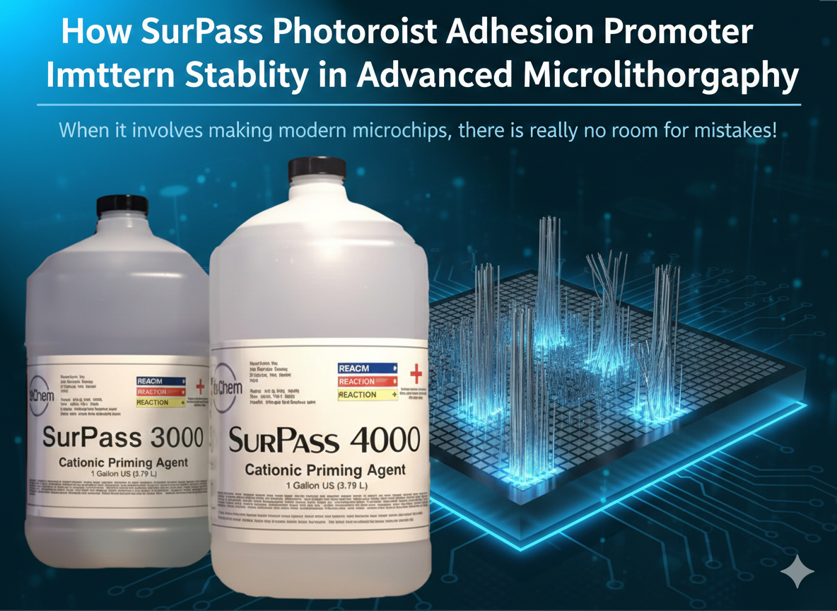
To solve this, DisChem offers surpass Adhesion Promoters. SurPass is an easy, water-based primer that you put on the wafer surface before you apply your coating. It helps the film stick firmly to the wafer, which stops your lines from falling over. This simple step saves lab time, stops waste, and yields huge savings in time and material costs.
A good chip factory relies on a variety of helpful chemicals. DisChem offers other simple and effective products for your lab.
Specialty Developers are high-purity washing liquids that clean away extra chemicals cleanly, leaving sharp, perfect edges on your tiny circuits.
Nickel Electroforming Chemistry provides premium metal-plating solutions that are exceptionally pure and coat surfaces evenly for plants making high-precision metal molds.
Using matching chemicals from one trusted supplier avoids mixing problems, makes buying simple, and keeps your overall operating costs low.
E-beam technology is vital for building AI chips because it offers the extreme precision needed to make tiny circuits. Even though it is slower than mass-production methods, it saves companies millions of dollars during the design phase. It eliminates the need for expensive stencils. By pairing this technology with DisChem’s reliable products, like H-SiQ resists, DisCharge H2O anti-static coatings, and SurPass primers, factories can prevent defects, save money, and build better tech.
At DisChem, we support high-precision scientific research and advanced nanomanufacturing across the region. If you want to integrate advanced lithography solutions, chemical resists, or specialized materials into your workflow, our technical experts are here to help.
Optical lithography uses ultraviolet light to project a chip pattern through a stencil mask. This is fast and perfect for mass production. E-beam lithography uses a narrow beam of electrons to draw patterns directly onto the surface. This offers much higher resolution but at a slower speed.
H-SiQ is a liquid glass resist that turns into a durable glass when exposed to an electron beam. This high-purity chemical structure prevents fine lines from falling over during development. This allows researchers to successfully print features under 10 nanometers.
When electrons hit glass or quartz, they pile up and create a negative charge. This charge bends the incoming electron beam, leading to pattern distortion and alignment errors. Using a conductive layer like DisCharge H2O safely conducts these electrons away.
SurPass primes the substrate surface before the resist is applied. This greatly enhances the bond between the resist and the wafer. This strong bond keeps ultra-fine, narrow lines standing upright and stable during the liquid washing and rinsing stages.